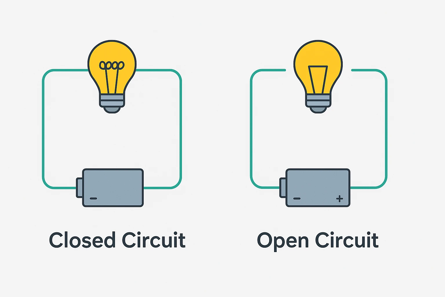
What is an Open Circuit?
An open circuit refers to a break or interruption in an electrical path that prevents current from flowing.
In simple terms, an open circuit occurs when the conductive path in a circuit is not complete—much like a disconnected wire or a missing connection on a PCB (Printed Circuit Board).
Definition of an Open Circuit
In electrical engineering, an open circuit is defined as a circuit where the continuity has been broken, meaning no current can pass through.
Even if a voltage source is applied, the absence of a closed path results in zero current flow. The resistance in an open circuit can be considered infinitely high.
Difference Between Open Circuit and Short Circuit
| Feature | Open Circuit | Short Circuit |
|---|---|---|
| Current Flow | No current flows | Excessive current flows |
| Resistance | Very high or infinite | Very low or zero |
| Common Cause | Disconnected wires, broken traces | Bridged wires, unintended paths |
| Impact | Device doesn't work | Can cause overheating or damage |
Understanding the difference between an open circuit and a short circuit is crucial for PCB troubleshooting and electrical safety.
Why Prevent Open Circuits Matter in PCB Manufacturing
In PCB design and manufacturing, open circuits are a common failure mode that can lead to malfunctioning devices, product recalls, or poor customer experience. These defects might be invisible to the naked eye but have significant impact on performance and reliability.
Typical causes of open circuits in PCBs include:
- Incomplete copper etching
- Poor via connections
- Cold or cracked solder joints
- Misalignment during layer stacking
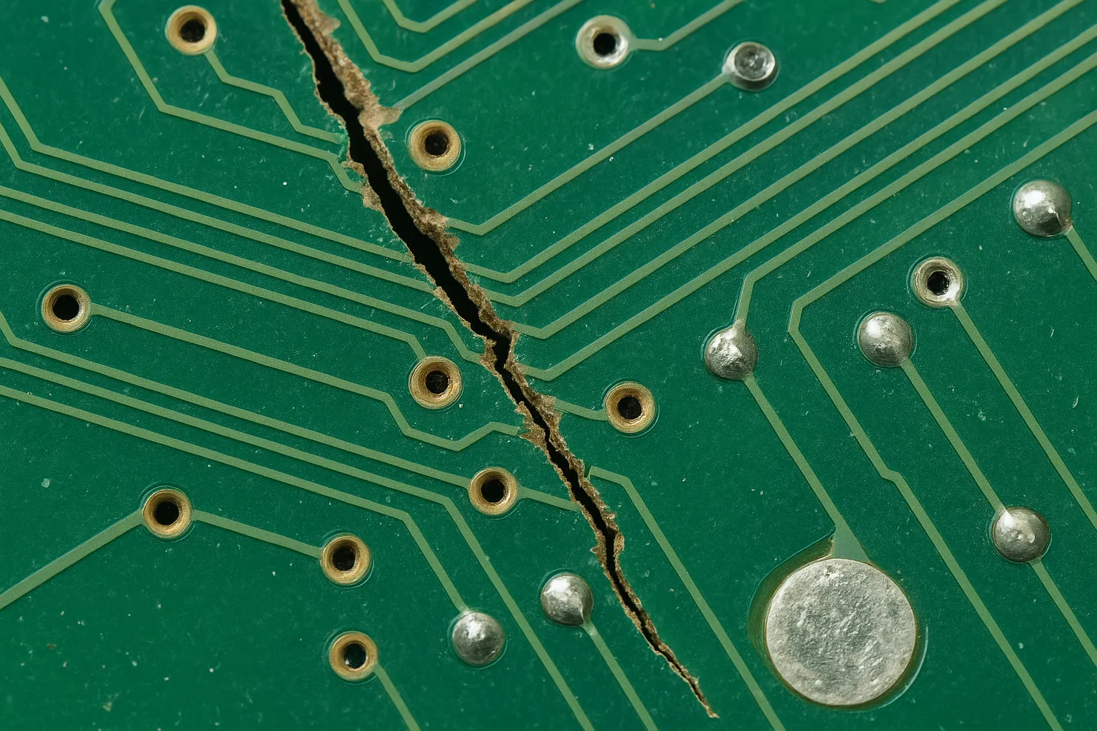
How Open Circuits Manifest in PCBs and Their Risks
In the world of printed circuit boards (PCBs), open circuits are a hidden but critical failure mode. These issues can cause electronic devices to malfunction, perform inconsistently, or stop working entirely.
Understanding how open circuits appear in PCBs—and the risks they pose—is essential for engineers, manufacturers, and quality control teams.
Common Symptoms of an Open Circuit in a PCB
Open circuits in PCBs may not always be visible to the naked eye, but they can trigger various functional failures. Here are some of the most common signs:
1. Device does not power on
An open trace or disconnected via in the power path can completely cut off current flow.
2. Intermittent operation
If the open circuit is caused by a cracked solder joint or micro-fracture, it might behave erratically—working sometimes and failing under vibration or thermal stress.
3. Non-responsive components
Microcontrollers, sensors, or LEDs might appear "dead" if their data or ground connections are open.
4. False or missing signals
In high-speed or analog circuits, an open line can result in signal loss, data corruption, or ghost readings.
5. No continuity during testing
In-circuit or flying probe tests often reveal open circuits through failed connectivity checks.
Why Open Circuits in PCBs Are a Serious Concern
1. Compromised Product Reliability
An open circuit can lead to early product failure, sometimes after the device has been shipped to customers. This severely impacts a brand's reputation and customer satisfaction.
2. Increased Cost Due to Rework or Scrap
Open circuits often require manual diagnostics, re-soldering, or complete board replacement—especially for densely populated SMT boards where access is limited.
3. Delayed Time-to-Market
Open circuit-related quality escapes during manufacturing or testing can delay product launches, especially if root cause analysis and corrective actions are needed.
4. Warranty Claims and Field Failures
If open circuits go undetected in production, they may lead to field returns, RMA (Return Merchandise Authorization) cases, and unexpected warranty costs.
Example: Open Circuit in Automotive PCB
Consider a brake system PCB with an open trace in the sensor feedback path. The brake may still engage, but the warning system will not trigger, creating a false sense of safety. This isn't just a quality issue—it's a safety-critical risk that could lead to liability and compliance failures.
Key Takeaway
Open circuits in PCBs are invisible threats with significant consequences. Even a single broken trace or cracked via can result in total or partial system failure.
That's why identifying, preventing, and resolving open circuits is a core focus in modern PCB manufacturing and quality assurance.
Common Causes of Open Circuits in PCB Manufacturing
In PCB fabrication and assembly, open circuits are among the most frustrating and costly defects. While often microscopic and hard to detect, they can stem from multiple points across the production process—from bare board etching to component soldering.
Understanding these root causes is key to preventing failures and improving yield and product reliability.
1. Etching Defects (Over-etching or Under-etching)
During the PCB manufacturing process, copper is etched away to form circuit traces. Improper etching—especially over-etching—can reduce trace width or even cut traces entirely.
- Cause: Inaccurate etching time, poor chemical concentration, or dirty resist film.
- Result: Broken or thinned copper traces, especially in high-density or fine-pitch designs.
2. Via and Hole Connection Failures
Multilayer PCBs rely on vias (through-holes, blind vias, buried vias) to create vertical electrical connections. If a via is not plated correctly, the signal path will break between layers.
- Cause: Incomplete copper plating, voids, contamination during electroplating.
- Result: Open circuit between internal or external layers.
3. Delamination or Layer Misalignment
If PCB layers are not precisely aligned during lamination, critical signal traces may not connect as intended, especially on multilayer boards.
- Cause: Mechanical shifting, press misalignment, uneven pressure.
- Result: Internal open circuits or inconsistent inter-layer connectivity.
4. Soldering Issues During SMT/Through-Hole Assembly
In the assembly phase, poor soldering can result in cold joints, solder voids, or incomplete wetting, all of which can create opens.
- Cause: Inconsistent reflow profile, poor solder paste application, component misplacement.
- Result: Intermittent or permanent opens, especially with leadless packages like BGA, QFN, or LGA.
5. Thermal or Mechanical Stress
Some opens develop after the PCB is produced, during testing or usage. These include cracked solder joints or trace breaks due to repeated mechanical stress or thermal cycling.
- Cause: PCB flexing, vibration, thermal expansion mismatch.
- Result: Micro-cracks leading to intermittent open circuits.
6. Design Issues and DFM Violations
Sometimes, open circuits are the result of flaws in the PCB design itself, such as missing vias, incorrect net routing, or lack of design-for-manufacturing (DFM) review.
- Cause: Incomplete netlists, missing copper connections, improper clearance.
- Result: Permanent opens baked into the board before it's ever built.
Summary Table: Root Causes of PCB Open Circuits
| Category | Example Cause | Typical Location | Prevention Tip |
|---|---|---|---|
| Etching Defect | Over-etched trace | Outer layers | Regular etching calibration |
| Via Failure | Incomplete plating | Multilayer interconnects | Use X-ray and micro-section analysis |
| Lamination Error | Layer shift during pressing | Inner layers | Tight lamination process control |
| Soldering Problem | Cold joint on QFN | Surface-mount pads | Profile optimization + AOI/ICT testing |
| Mechanical Stress | Board flexing in assembly | High-strain regions | Use strain relief and reinforced layout |
| Design Error | Missing via in net | Schematic/layout | DFM review with experienced engineers |
Takeaway
often preventable when proper controls are applied at every stage—from design to final assembly.
Whether it's trace width control during etching or thermal profile tuning during reflow, each step plays a role in ensuring electrical continuity and final product quality.
How to Detect and Diagnose Open Circuit Issues in PCBs
Open circuits in printed circuit boards (PCBs) can be elusive and costly if left undetected.
Fortunately, modern inspection and testing methods allow manufacturers to pinpoint these defects during or after production. Early detection is essential to avoid product failures, rework costs, or customer returns.
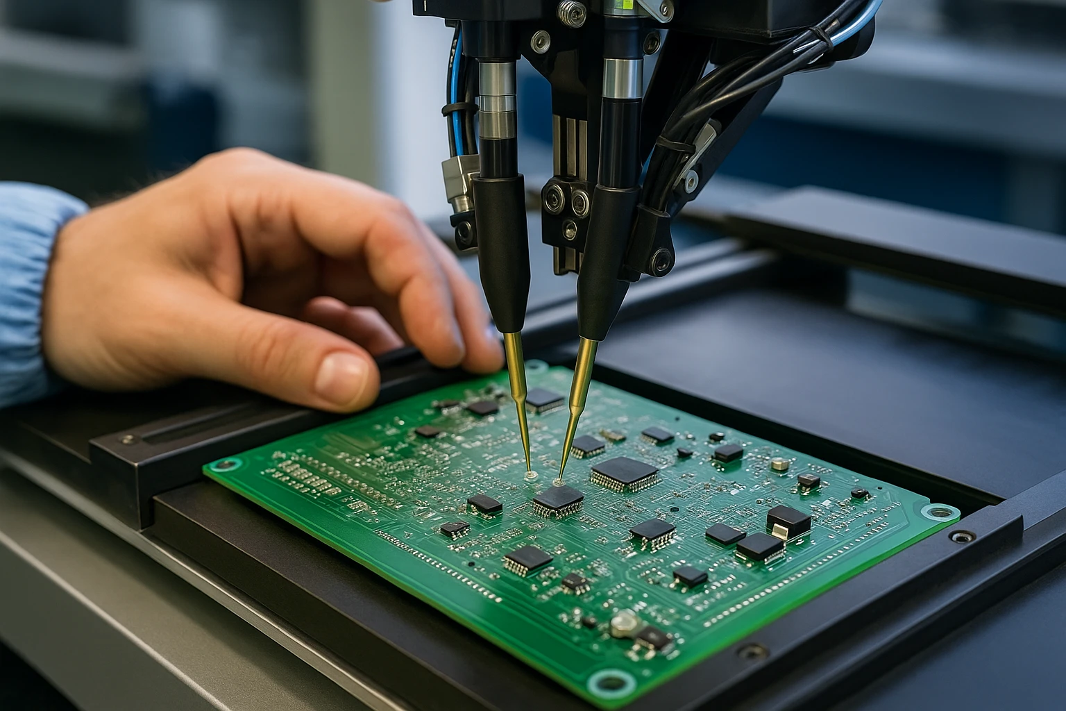
1. Continuity Testing (Manual or Automated)
The most basic method for detecting open circuits is continuity testing, which checks whether electricity can flow between two points.
- Tools: Multimeter (manual), continuity testers, or embedded test software.
- Use Case: Ideal for simple circuits or prototypes.
- Limitation: Not scalable for high-volume or high-complexity boards.
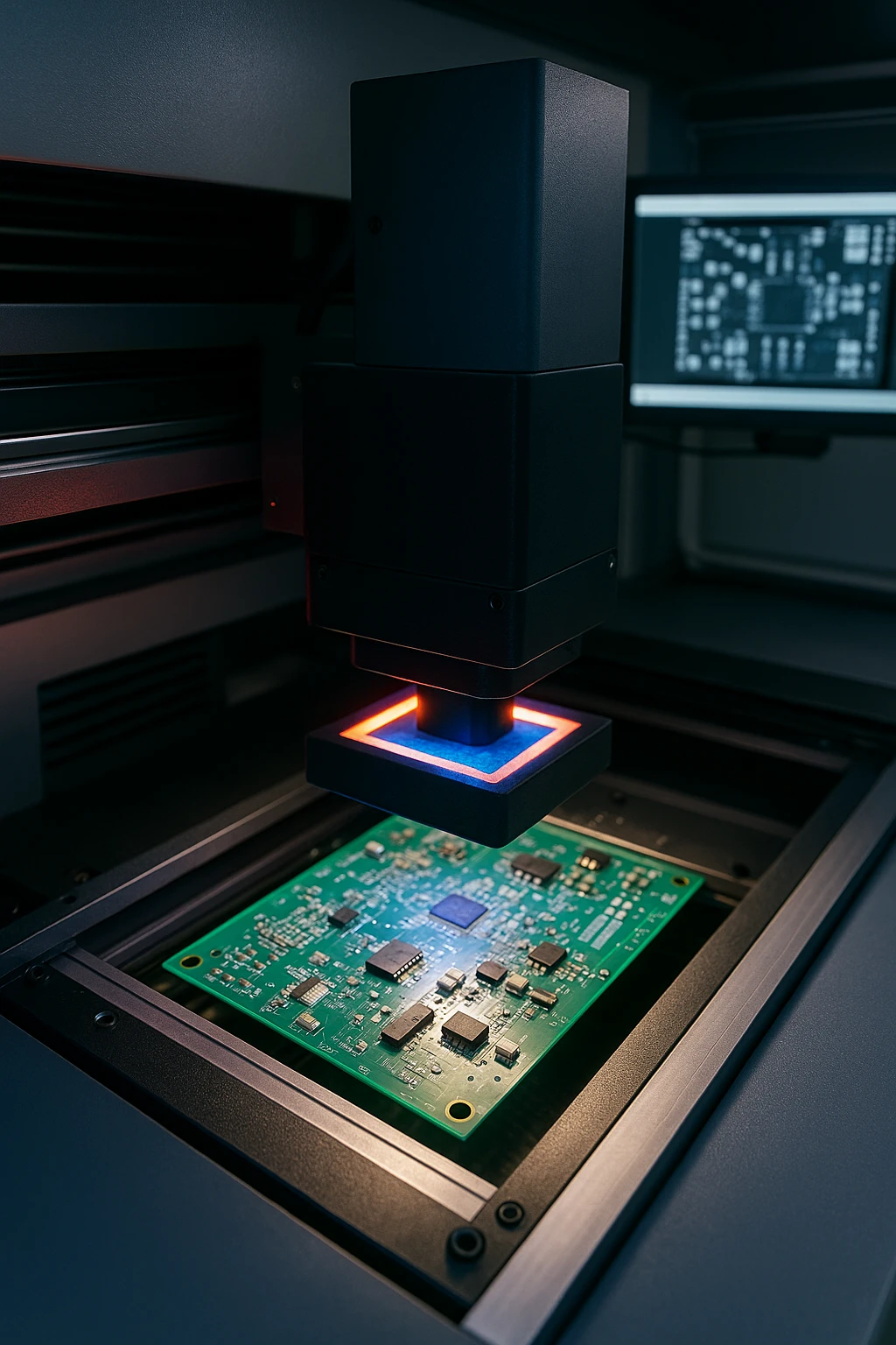
2. Flying Probe Testing (FPT)
Flying probe testers use movable probes to test electrical connectivity across the board without a physical test fixture.
- Advantages:
- No need for custom fixtures
- Suitable for low- to mid-volume production
- Can test fine-pitch and high-density boards
- What It Detects: Opens, shorts, component orientation, missing nets
- Limitation: Slower than ICT for large-scale production
3. In-Circuit Testing (ICT)
ICT is a bed-of-nails type test that checks the integrity of circuits, components, and connectivity using a fixture.
- Advantages:
- Fast, repeatable, and highly accurate
- Detects open circuits, cold solder joints, and missing components
- Use Case: Best for high-volume production with stable designs
- Limitation: Requires custom fixture, longer setup time
4. Automated Optical Inspection (AOI)
AOI uses high-resolution cameras and image processing to detect visible surface defects.
- Detects:
- Missing solder
- Misaligned components
- Visible cracks or incomplete solder joints
- Limitation: Cannot detect internal open circuits or hidden defects
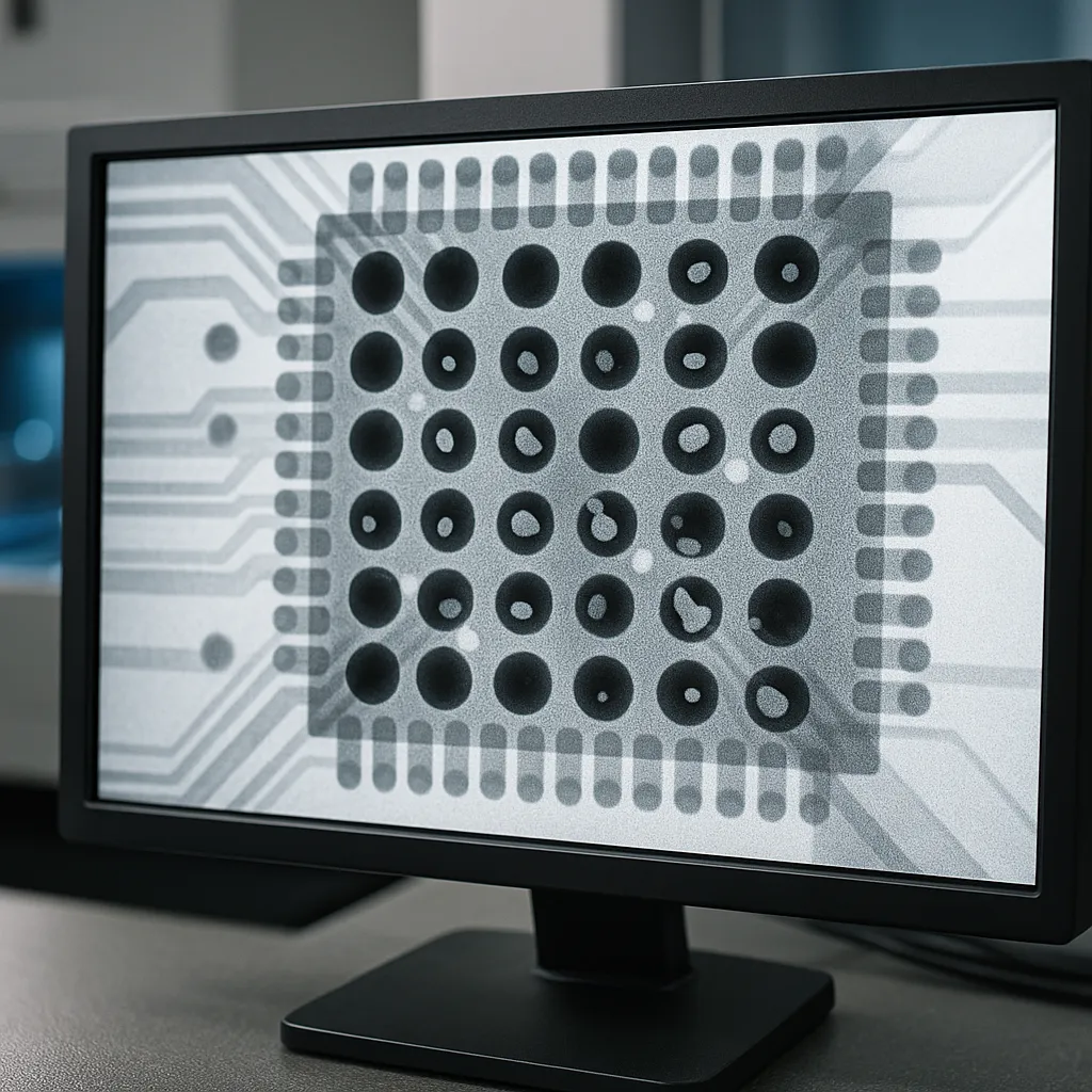
5. X-ray Inspection (AXI)
For hidden solder joints such as BGAs, QFNs, or inner vias, X-ray imaging is essential.
- Use Case: Detects voids, cold solder joints, and incomplete connections not visible from the surface
- Limitation: High equipment cost and requires trained operators
6. Functional Testing (FCT)
In functional testing, the PCB is powered on, and its behavior is checked under simulated real-world conditions.
- Detects: Any failure in power delivery, data transmission, signal logic, or I/O communication—often due to open circuits
- Best Used For: Final validation before shipment
- Limitation: Does not reveal root cause unless combined with diagnostic tools
Bonus Tip: Use Combined Testing Strategies
Most professional PCB manufacturers use a combination of the above methods to achieve optimal test coverage. For example:
- AOI → ICT → FCT
- Flying probe → X-ray → Functional test
This layered approach ensures both visual and electrical integrity, increasing reliability and reducing the risk of latent open-circuit failures in the field.
Summary Table: Detection Techniques for PCB Open Circuits
| Method | Detects Open Circuits | Speed | Ideal For | Limitations |
|---|---|---|---|---|
| Multimeter | ✔️ (manual) | Slow | Prototypes, lab work | Not scalable |
| Flying Probe Test | ✔️ | Moderate | Low-mid volume | Slower for large batches |
| In-Circuit Test (ICT) | ✔️ | Fast | High-volume production | Requires fixture |
| AOI | ✔️ (surface only) | Fast | SMT, visual defects | Can’t detect hidden opens |
| X-ray Inspection | ✔️ (internal) | Moderate | BGA, QFN, complex PCBs | Costly, image interpretation |
| Functional Test (FCT) | ✔️ (indirectly) | Moderate | Final product validation | Needs full system logic testing |
Takeaway
Detecting open circuits is not just about using one tool—it's about combining technologies to find both visible and invisible faults.
Whether through flying probe tests, in-circuit testing, or X-ray inspection, thorough testing ensures electrical continuity, product safety, and customer satisfaction.
Prevention and Quality Control Strategies for Avoiding Open Circuits in PCB Manufacturing
Open circuits in PCBs can lead to costly repairs, functional failures, and reputational damage. Fortunately, with the right preventive measures and quality control systems in place, manufacturers can significantly reduce the risk of open circuits occurring during the production lifecycle.
This section outlines practical, proven strategies to prevent open circuits from the early design phase to final inspection.
1. Design for Manufacturability (DFM) Review
Many open circuits originate from the design stage. Applying DFM principles helps ensure the layout is optimized for both manufacturability and reliability.
- Best Practices:
- Use correct trace width, via size, and spacing
- Ensure complete netlist and proper grounding
- Minimize trace crossovers and complex routing
- Tools: DFM analysis software, Gerber validation tools, schematic/layout checks
2. Tight Process Control During Etching and Plating
Over-etching and poor copper plating are major causes of broken traces and incomplete vias.
- Etching Controls:
- Regularly calibrate chemical concentrations and etching time
- Use test coupons to verify trace integrity
- Plating Controls:
- Ensure uniform copper thickness
- Use micro-section analysis to check via wall quality
3. Multistage In-Process Inspection
Implementing multiple inspection points across the production line ensures early detection and correction of open circuits.
- Critical Checkpoints:
- Post-etch AOI (detect trace gaps)
- Pre- and post-lamination alignment checks
- Post-reflow AOI for solder joint validation
- Technologies: AOI, ICT, flying probe, X-ray
4. Optimized Soldering and Reflow Profiles
Improper soldering is one of the leading causes of open joints in SMT assemblies, especially for BGAs and QFNs.
- Preventive Measures:
- Calibrate reflow ovens for accurate temperature curves
- Monitor solder paste deposition and stencil wear
- Use nitrogen atmosphere for improved wetting
- Inspection After Soldering:
- Perform X-ray inspection for hidden joints
- Use FCT to verify full circuit functionality
5. Robust Quality Management System (QMS)
A structured QMS helps enforce repeatability, traceability, and accountability in production.
- Standards to Follow:
- IPC-A-600 for PCB acceptability
- ISO 9001 or IATF 16949 for system quality
- IPC-A-610 for assembly workmanship
- Best Practices:
- Document inspection results digitally
- Train technicians with updated guidelines
- Use statistical process control (SPC) to monitor variation
Bonus: Collaborate with High-Reliability Suppliers
Prevention doesn't end within your factory. Working with qualified material suppliers (e.g., high-quality laminate, solder paste, and plating chemicals) can drastically reduce risk at the source.
- Audit supplier quality systems
- Request process capability reports (CPK)
- Ensure proper storage and handling of sensitive materials
Final Takeaway
Preventing open circuits requires a holistic approach—starting from thoughtful design and continuing through controlled manufacturing, rigorous inspections, and supplier partnerships.
By building preventive practices into every stage, you not only reduce defects but also build trust with customers who demand reliability and performance.
Our Technical Advantages in Preventing Open Circuits
As a professional PCB manufacturer and assembly provider, our commitment to quality begins long before production—and extends throughout the entire process.
We have developed a set of technical capabilities, process innovations, and inspection protocols that directly address and prevent open circuit failures across a wide range of PCB applications.
Here's how we ensure maximum electrical continuity and product reliability:
1. Design-for-Manufacturing (DFM) Collaboration with Clients
We work closely with clients during the PCB layout phase to help them optimize for manufacturability and reduce risk of open circuits.
- DFM reviews of trace width, via size, and layer stackup
- Automated Gerber file checking to catch missing or disconnected nets
- Pre-manufacturing simulations to validate impedance and signal integrity
2. Advanced Fabrication Equipment and Tight Process Control
Our factory utilizes automated, high-precision fabrication tools with built-in monitoring and process tracking.
- Laser direct imaging (LDI) for ultra-precise pattern alignment
- Controlled etching and plating lines with inline thickness sensors
- Layer registration systems to eliminate stack-up misalignment
3. Multi-Tiered Inspection Systems Across the Workflow
We employ a layered inspection strategy that ensures any potential open circuit is caught early and eliminated.
- AOI (Automated Optical Inspection) after etching and soldering
- Flying Probe Testing for sample-based electrical verification
- 100% In-Circuit Testing (ICT) for high-volume orders
- Optional X-ray for BGA and hidden-joint verification
4. Custom Reflow Profile Tuning for High-Reliability Soldering
Open circuits often stem from poor soldering. We fine-tune reflow profiles for each assembly to guarantee full wetting and joint integrity.
- Custom thermal profiling for each BOM and stackup
- Real-time solder paste inspection (SPI)
- Nitrogen reflow options for sensitive boards and lead-free solder
5. Strict Compliance with International Standards
All our manufacturing and assembly processes conform to globally recognized quality standards.
- IPC-A-600 (PCB acceptance), IPC-A-610 (assembly workmanship)
- ISO 9001 and ISO 13485 certified facilities
- Optional IPC Class 3 production for mission-critical applications (e.g. aerospace, medical)
6. Real-Time Quality Monitoring and Full Traceability
We integrate real-time SPC (Statistical Process Control) and MES (Manufacturing Execution System) monitoring to detect any variation before it causes a failure.
- Lot-based traceability down to batch, panel, and reel level
- Quality dashboards showing yield trends and inspection flags
- Root cause analysis and CAPA tracking for any issue found
Why It Matters
These technical advantages allow us to deliver low-defect-rate PCBs that meet the demands of industries where failure is not an option—such as automotive, medical, telecom, and industrial automation. Our systematic approach to preventing open circuits ensures consistent performance, long-term durability, and peace of mind for our customers.
Ready to eliminate open circuit failures and ensure the electrical integrity of your next PCB project?
Partner with a manufacturer that combines advanced process control, multi-layer inspection systems, and design-for-manufacturing expertise.