


In multilayer printed circuit board (Multilayer PCB board) manufacturing, the stack-up structure is one of the most critical factors affecting performance, cost, and reliability.
The Type 3 multilayer stack-up is the most fundamental configuration and is the basis of most modern PCB fabrication.
This article explains how Type 3 Multilayer PCB boards are constructed, the materials involved, and the three main lamination methods—copper-foil outer layers, core-based outer layers, and odd-layer stack-ups—along with their design logic, pros, and cons.
What Is a PCB Stack-Up?
A stack-up is the layer-by-layer arrangement of copper foils, dielectric materials, and cores that form a Multilayer PCB board.
It defines both the electrical performance (impedance, signal integrity) and mechanical stability (warpage, adhesion strength) of the finished board.
In a Type 3 structure, three key materials are used:
- Copper-clad laminate (Core): A C-stage (fully cured) fiberglass epoxy board clad with copper on both sides, used for internal layers.
- Prepreg: A B-stage (partially cured) resin sheet that bonds layers together and fills voids between copper traces.
- Copper foil: Used to form outer-layer circuits, pads, and ground planes.
According to IPC-2221 and IPC-2222, designers must define the resin system, glass-cloth type, and dielectric tolerances in the documentation to ensure mechanical and electrical compliance.
Type 3 Stack-Up with Copper Foil Outer Layers — The Mainstream Design
The most common Type 3 structure uses copper foil as the outer layers.
It is built by laminating several inner cores (each already etched with circuit patterns) together with two sheets of copper foil and layers of prepreg.
Typical Example: Eight-Layer Board
An 8-layer Type 3 Multilayer PCB board usually consists of:
- Three copper-clad cores (inner layers already imaged and etched);
- Two sheets of copper foil for the top and bottom;
- Prepreg layers between each core.
Layer numbering runs from L1 (top) to L8 (bottom):
- L2, L4, L5, and L7 are signal layers;
- L3 and L6 are power/ground planes;
- L1 and L8 are outer circuit layers with component pads and fan-out vias.
When thick copper (2 oz or more) is used for signal layers, high-resin prepreg should be placed next to those layers to ensure full resin fill and avoid voids during lamination.

Advantages
- Low material cost – Copper foil and prepreg are cheaper than full core laminates.
- Reduced chemical consumption – Less photoresist and etchant required.
- Lower labor cost – Fewer pre-lamination and imaging steps.
- High yield – Simple process with mature manufacturing control.
Due to its excellent cost-performance, the copper-foil outer-layer stack-up is the most economical and widely used in mass production.
Type 3 Stack-Up with Core-Based Outer Layers — For High-Precision Needs
Another Type 3 configuration uses copper-clad cores for the outer layers instead of copper foil.
It follows the same overall principle but changes the lamination and imaging order.
Structural Characteristics
For the same 8-layer board:
- This version uses four cores instead of three;
- The outer layers do not use B-stage prepreg or copper foil;
- One side of each outer core is imaged and etched before lamination, while the opposite side remains copper-clad;
- After lamination, the untouched outer sides are then imaged to form the final outer circuits.
Design Logic
This structure allows L3 and L6 to pair with signal layers for better dielectric-thickness and impedance control, which is crucial in high-frequency or high-voltage applications.
Advantages
- Improved surface planarity – Reduces weave texture or “print-through” patterns that may appear on outer traces when thick copper is used.
- Enhanced dielectric control – Fully cured (C-stage) cores have tighter thickness tolerances than prepreg layers.
- Optimized process flow – Useful when ultra-thin cores are required or when maintaining symmetry is difficult.
Disadvantages
- Lower yield – Outer copper surfaces require repeated protection and cleaning through etching, stripping, and brown-oxide steps, increasing scratch risk.
- Higher material and labor cost – Additional cores and handling steps raise total cost.
- More complex manufacturing – Demands tighter process control.
Therefore, this stack-up is used mainly for high-end Multilayer PCBs where flatness and impedance precision outweigh cost.
Odd-Layer Stack-Up Structures — Special Case for Signal Spacing
When circuit design calls for larger dielectric spacing or an odd number of layers, manufacturers can adopt an odd-layer stack-up using a single-sided copper-clad laminate as one outer layer.
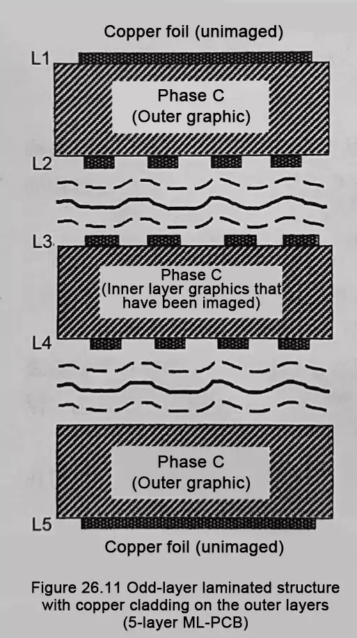
Material Preparation
- Commercial single-sided cores are easy to obtain but have poor bonding strength on the bare (non-copper) side.
Surface roughening or special chemical treatment is required. - Alternatively, one side of a double-sided core can be etched away, leaving a rough copper “tooth” structure that improves adhesion during lamination.
Engineering Considerations
- Enables odd-layer circuit designs;
- Offers more flexibility in dielectric spacing for specific signal or impedance needs;
- However, maintaining mechanical balance is critical to prevent board warpage.
Balancing Techniques
Using symmetrical core thickness and even dielectric distribution helps achieve structural stability.
In Multilayer PCB board fabrication, especially for large or thin boards, stack-up symmetry is a key factor in yield and reliability.
Stack-Up Design and Signal Integrity
No matter which lamination method is used, signal integrity (SI) depends heavily on the stack-up design.
The spacing, dielectric constant, and arrangement between signal and ground layers directly determine impedance, crosstalk, and EMI performance.
A well-designed Type 3 stack-up:
- Minimizes crosstalk between traces;
- Provides stable return paths;
- Ensures consistent impedance across layers.
- Improves overall electromagnetic compatibility.
In other words, stack-up design is the first step in signal-integrity planning, not a correction after routing.
Summary — Balancing Cost, Reliability & Performance
The Type 3 Multilayer PCB board stack-up remains the backbone of the industry.
By choosing the right outer-layer method—copper foil, core-based, or odd-layer—engineers can balance cost, reliability, and performance according to project needs.
| Copper-foil outer layers | Low cost, high yield | Moderate impedance control | General-purpose boards, mass production |
| Core-based outer layers | Excellent flatness, precise impedance | Higher cost, complex process | High-frequency or high-reliability Multilayer PCB boards |
| Odd-layer stack-up | Supports special signal spacing | Harder to control warpage | Custom or experimental designs |
Final Thoughts
A PCB stack-up isn’t just a pile of materials—it’s a design philosophy that defines both electrical performance and mechanical integrity.
Mastering the principles of the Type 3 Multilayer PCB board structure is essential for understanding advanced HDI and next-generation interconnect technologies.
