


What Is a Metal Core PCB (MCPCB)?
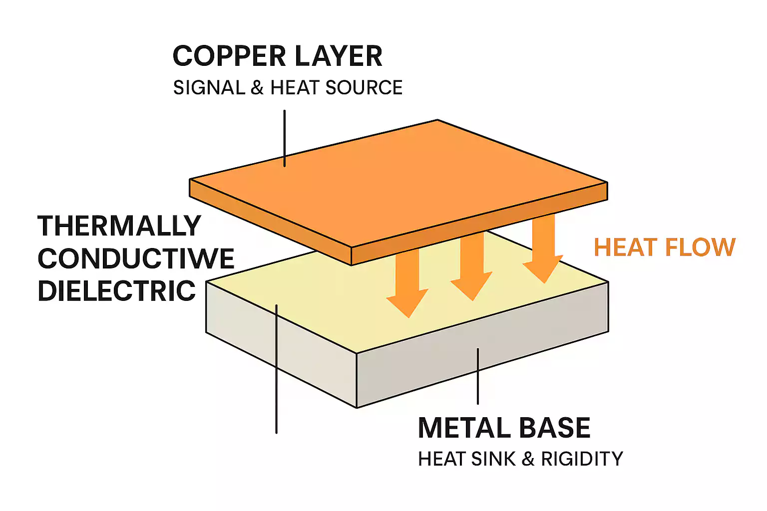
A Metal Core PCB (MCPCB)—also called metal-clad PCB or insulated metal substrate (IMS) PCB—is a printed circuit board built on a metal base (usually aluminum or copper) with a thin, thermally conductive, electrically insulating dielectric between the metal and the copper circuit layer. The goal is simple: move heat away from components faster than standard FR-4 can, while keeping everyday PCB manufacturing and assembly workflows.
How an MCPCB Is Built (Layer Stack)
Think of a sandwich, from bottom to top:
- Metal base (aluminum is most common; copper for maximum heat spreading)
- Thermally conductive dielectric (electrically insulating “glue” that bonds metal to copper and provides a low thermal-resistance path)
- Copper foil (the circuit layer: 1–3 oz typical, heavier copper possible)
- (Optional) Solder mask and surface finish (ENIG, OSP, etc.)
Typical dimensions (for orientation, not hard limits):
- Metal base thickness: often 1.0–3.2 mm (aluminum most common)
- Dielectric thickness: often ~75–150 µm to balance isolation and low thermal resistance
- Dielectric thermal conductivity: commonly 1–3+ W/m·K depending on material grade
Why the Structure Matters
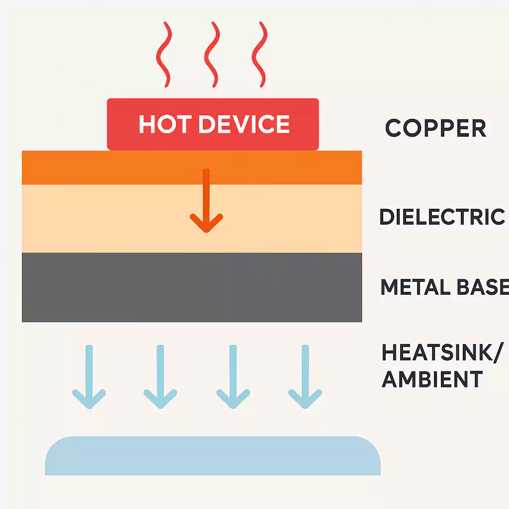
- Fast vertical heat path: Heat flows from hot devices → copper → dielectric → metal base → heatsink/ambient.
- Lower board temperature: Reduces junction temperature (Tj), improving LED lumen maintenance, power device reliability, and overall MTBF.
- Mechanical rigidity: The metal base adds stiffness and acts as a built-in heat spreader.
MCPCB vs. “Metal-Clad PCB” vs. “Aluminum PCB” vs. “IMS”
- MCPCB / Metal-Clad PCB / IMS PCB: Generally interchangeable in the industry, these terms describe a metal-based PCB with an insulating dielectric layer beneath the copper circuits.
- Aluminum PCB: A subset of MCPCB using an aluminum base (the most popular, cost-effective choice).
- Copper-core PCB: Another subset utilizing copper as the base for optimal heat dissipation (higher cost and weight).
Common Form Factors
- Single-layer MCPCB (most used): One copper layer on the dielectric. Ideal for high-power LEDs, drivers, and PSU modules.
- Double-layer MCPCB: Two copper layers on the dielectric; routing flexibility improves, but requires via isolation techniques to avoid shorting to the metal.
- Multilayer MCPCB: Possible but more complex/costly; used when both thermal and dense routing needs must be met. In advanced builds, special processes (e.g., extensive drilling, insulating fill, and re-drilling before plating) keep plated-through vias isolated from the metal base.
When to Use MCPCB (Applications)
Use a metal core PCB when heat density—not routing density—is your main constraint. Typical, high-value use cases:
- LED lighting (backlight, general, COB/CSP)
- Why MCPCB: Keeps junction temperature low for lumen maintenance and color stability.
- Design hint: Single-layer aluminum base with 1–3 W/m·K dielectric is the default; spread heat with short, wide copper pours.
- Automotive lighting & e-powertrain controllers
- Why: Elevated ambient, vibration, and long duty cycles demand predictable thermal paths.
- Hint: Thicker base metal for stiffness; verify creepage/clearance and mounting hole isolation.
- Motor drives & motion control
- Why: Hot power FETs/IGBTs and shunt resistors cluster together.
- Hint: Place hot devices directly over the metal core; consider copper base when hotspots persist.
- Power supply devices (AC/DC, DC/DC, LED drivers)
- Why: Continuous dissipation and compact layouts make FR-4 + clip-on heatsinks marginal.
- Hint: Use higher-k dielectric or thinner dielectric to reduce component-to-base thermal resistance.
- Solid-state relays & load switches
- Why: Pulsed/steady thermal loads benefit from a short, consistent conduction path.
- Hint: Keep SMT-only where possible; isolate any required vias from the metal base.
- Solar/PV and power conditioning modules
- Why: Harsh environments and enclosure heating raise board temperatures.
- Hint: Aluminum base for cost/performance; seal edges and mounting to prevent corrosion ingress.
- Industrial & RF power (laser drivers, PA modules)
- Why: Heat flux and stability beat complex TIM stacks.
- Hint: Use MCPCB as an integrated heat spreader to simplify mechanics and improve repeatability.
Material Comparison: Aluminum vs Copper
Metal core PCBs (MCPCBs) most commonly use aluminum or copper bases. Your choice drives thermal performance, weight, cost, and manufacturability.
| Property | Aluminum (5052/6061) | Copper (C110) | What it means for MCPCB |
|---|---|---|---|
| Thermal conductivity (k) | ~150–205 W/m·K | ~385–400 W/m·K | Copper spreads heat 2× faster—useful for tight hotspots. |
| Density / Weight | 2.7 g/cm³ (light) | 8.9 g/cm³ (heavy) | Copper bases can triple board weight—watch for mass limits. |
| CTE (in-plane) | ~23 ppm/°C | ~16–17 ppm/°C | Copper’s CTE is closer to copper circuitry and many packages, improving joint stability under cycling. |
| Cost (material + machining) | Low | High | Copper base adds noticeable cost from raw metal and tool wear. |
| Machinability | Easy; fast routing/drilling | Tough; higher tool wear | Aluminum favors short lead time and lower NRE. |
| Stiffness at equal thickness | Good | Very good | Copper can be thinner for the same stiffness but still heavier. |
| Corrosion behavior | Oxides quickly; anodize/paint edges | Tarnishes; generally stable | Protect aluminum edges and mounting points to prevent galvanic issues. |
MCPCB Stackups That Work
The performance and manufacturability of a metal core PCB depend heavily on how it’s stacked up—how layers of copper, dielectric, and metal substrate are arranged and connected. Choosing the right MCPCB stackup helps optimize thermal transfer, electrical performance, and production cost.
1. Single-Layer MCPCB (Most Common for LED Modules)
- Structure:
Copper foil → Dielectric layer → Metal base (Aluminum/Copper) - Use case: LED PCBs, driver circuits, low-complexity power boards
- Advantages:
- Simplest and most cost-effective stackup
- Excellent thermal path for surface-mounted components
- Ideal for mass production
2. Double-Layer MCPCB (2-Layer Copper with One Solder Side)
- Structure:
Top copper layer → Dielectric → Bottom copper layer (via through-holes or blind vias) → Dielectric → Metal base - Use case: Circuits requiring signal routing + power handling
- Advantages:
- Allows for more complex routing than single-layer
- Top side used for components; bottom copper for grounding or heat spreading
- Manufacturing note: Vias must be insulated from the metal base to prevent shorting.
3. Multilayer MCPCB with Insulated Vias (For High Power + Complex Logic)
- Structure:
Multi-copper layers on FR-4 → Thermally conductive dielectric → Metal base - Use case: Power modules with control logic, industrial automation, automotive ECUs
- Advantages:
- Combines thermal performance with complex circuitry
- Enables top/bottom side mounting, better signal integrity
- Challenges:
- Higher cost and manufacturing complexity
- Requires thermal via arrays and metal base isolation strategies
Thermal Design Essentials
Thermal management is the primary reason to choose a metal core PCB (MCPCB). A well-designed thermal path keeps junction temperatures low, extends component life, and avoids costly system-level cooling.
How Heat Flows in an MCPCB
The MCPCB stack is designed to move heat vertically from hot components into the metal base. The thermal path is:
Component → Copper → Dielectric → Metal Core → Heatsink or Ambient
Each layer has its own thermal resistance, and the total resistance affects the temperature rise.
Thermal Resistance Formula
Use this simplified formula to estimate the total board-level thermal resistance (Rθ_total, in °C/W):
[Rθ{total} = \frac{t{Cu}}{k_{Cu} \cdot A} + \frac{t_{dielectric}}{k_{dielectric} \cdot A} + \frac{t_{metal}}{k_{metal} \cdot A}]
Where:
- t = thickness of each layer (in meters)
- k = thermal conductivity (in W/m·K)
- A = heat transfer area (in m²)
In most MCPCBs, the dielectric layer dominates thermal resistance due to its low k-value.
Typical Values (Reference)
| Layer | Thickness (typ.) | Thermal Conductivity (k) | Contribution to Rθ |
|---|---|---|---|
| Copper | 35–70 µm | 385 W/m·K | Minimal |
| Dielectric | 100–150 µm | 1–5 W/m·K | High |
| Metal Base | 1.0–3.2 mm | Al: 200, Cu: 400 W/m·K | Low |
DFM Design Rules for Metal Core PCBs
Design for Manufacturability (DFM) is critical when working with metal core PCBs (MCPCBs), as thermal performance, isolation requirements, and base material rigidity all impact what can be reliably fabricated. Following these design rules ensures higher yields, better thermal performance, and lower costs.
1. Minimum Design Parameters
| Feature | Typical Value | Notes |
|---|---|---|
| Trace width/spacing | ≥ 6 mil (150 µm) | Wider preferred for thermal/current flow |
| Minimum hole size | ≥ 12 mil (0.3 mm) | Avoid very small vias due to metal base drilling |
| Annular ring | ≥ 5 mil (125 µm) | Larger for isolated plated-through holes |
| Dielectric thickness | 75–150 µm | Thinner = better heat transfer, but harder to isolate |
| Copper thickness | 1–3 oz (35–105 µm) | Up to 6 oz possible for high current |
| Base metal thickness | 1.0–3.2 mm | Aluminum 1.5 mm is standard for LED; copper heavier |
| Solder mask clearance | ≥ 3 mil (75 µm) | Adjust for thermal pad alignment |
| Silkscreen clearance | ≥ 5 mil from pads | Avoid print on heat-conductive areas |
2. Via Isolation Best Practices
- Do not allow through-hole plating to come into contact with fill/plugthe metal base. Use large clearance holes in the metal and filled/plugged vias for safe routing.
- Use non-conductive epoxy fill for plated vias passing near the base—especially in multilayer or double-sided MCPCBs.
3. Stackup and Layering Tips
- For single-layer MCPCBs: place all components on one side; use the metal base for thermal sinking only.
- For two-layer or multilayer: define via keep-out zones around critical thermal paths and high-voltage nets.
- Choose a dielectric material with known thermal conductivity (e.g., 1–3 W/m·K) and abreakdown voltage ≥ 3 kV for power circuits.
4. Surface Finish Recommendations
- OSP or ENIG are commonly used; ENIG preferred for high-reliability and fine-pitch components.
- Avoid HASL where flatness or precise pad geometry is required, especially with thermal pads.
MCPCB vs Other PCB Technologies
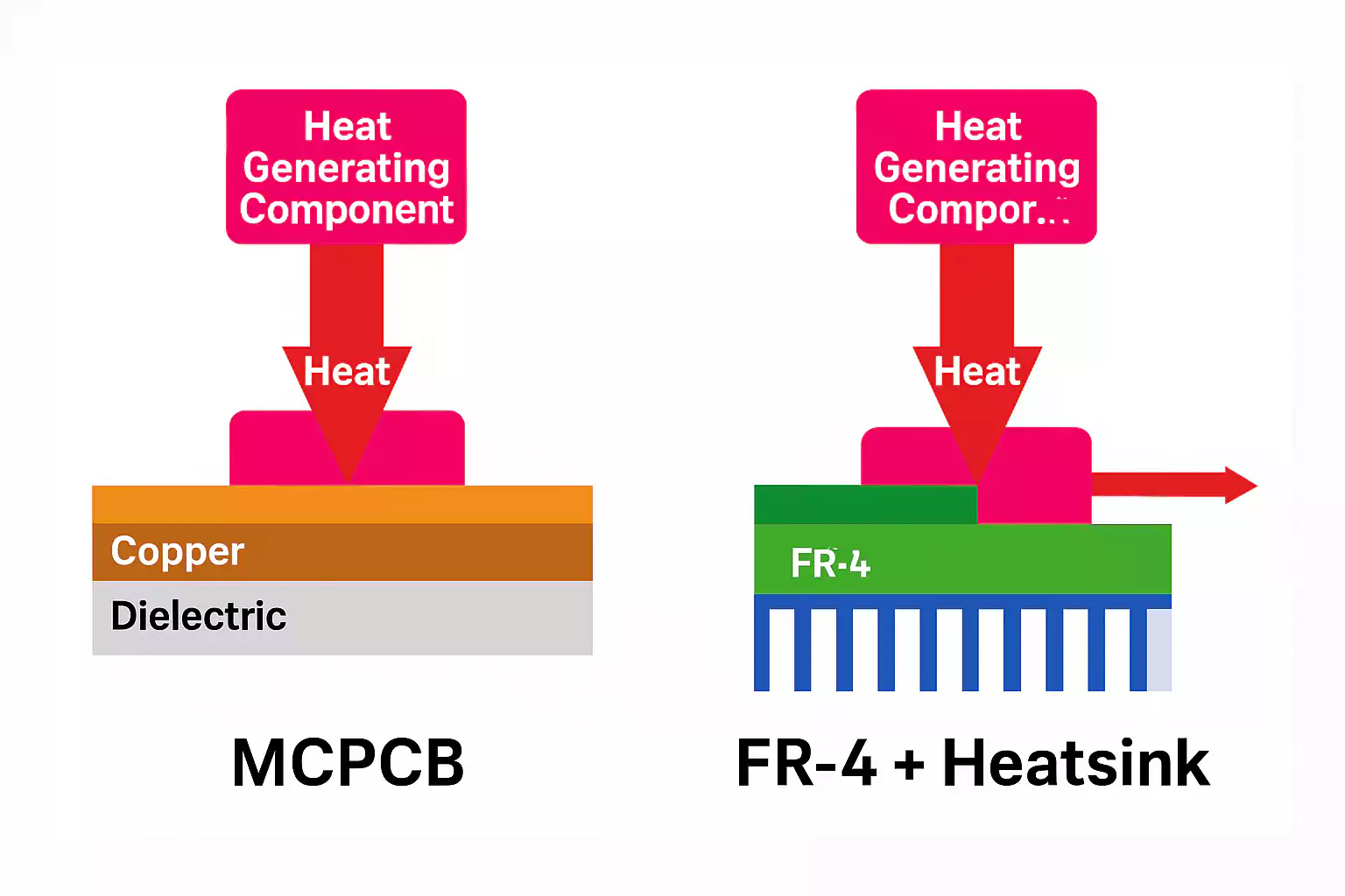
| Feature / Property | MCPCB | FR-4 + Heatsink | Ceramic PCB | Thick Copper PCB |
|---|---|---|---|---|
| Thermal Conductivity | ★★☆ (1–10 W/m·K) | ★☆☆ (Low, depends on TIM) | ★★★ (20–180 W/m·K) | ★★☆ (Lateral, not vertical) |
| Heat Path Efficiency | Vertical, direct-to-metal base | Indirect, multi-interface | Vertical, through ceramic | Lateral spread through copper |
| Operating Temperature | Up to ~130–150°C | Up to ~120°C | Up to ~250°C+ | Up to ~180°C |
| Cost | $$ (moderate) | $$–$$$ (depends on heatsink) | $$$$ (high) | $$$ (copper cost + process) |
| Mechanical Strength | Rigid (metal base) | Moderate | Brittle | Rigid |
| Manufacturing Complexity | Standard PCB + isolation steps | Simple PCB + manual assembly | Specialized, limited supply base | Complex etching/plating |
| Best For | LED, power, automotive modules | Consumer electronics with airflow | High-temp, high-power RF, lasers | High-current industrial power |
Conclusion
Metal core PCBs offer a proven solution for managing heat in high-power and thermally sensitive electronic designs. By integrating a thermally conductive metal base directly into the PCB structure, MCPCBs provide faster heat transfer, better thermal control, and simplified mechanical design—especially compared to traditional FR-4 or more costly ceramic substrates.
Whether you're designing LED modules, motor controllers, or power converters, MCPCBs can help:
- Lower junction temperatures
- Improve system reliability and lifetime
- Reduce the need for bulky heatsinks or complex cooling assemblies
- Streamline manufacturing with fewer parts and simpler assembly
With the right material selection, stackup, and DFM-aware layout, MCPCBs are not just a thermal solution—they're a strategic advantage in modern electronic products.
