


Printed Circuit Boards (PCBs) are the foundation of all modern electronics, but not all boards are built the same. Industrial PCB manufacturing focuses on creating boards that can withstand extreme environments, operate continuously, and meet higher reliability demands. From material selection to testing and certification, every step in industrial PCB production is held to tighter tolerances and stricter quality controls.
This guide explains what makes industrial PCBs distinct, outlines the key manufacturing processes and standards, and offers insight into selecting the right supplier for your next industrial project.
What Is “Industrial” PCB Manufacturing?
Industrial PCB manufacturing refers to the design and fabrication of circuit boards used in industrial-grade equipment—such as factory automation, robotics, power conversion, and control systems. These boards operate under high temperature, vibration, moisture, and electrical stress for long periods, often 24/7.
Unlike consumer electronics, which prioritize cost and compactness, industrial PCBs emphasize durability, reliability, and traceability. Components are chosen for extended temperature ranges (-40°C to +125°C), boards are reinforced with thicker copper and stronger laminates, and testing is performed more extensively.
Industrial PCBs must maintain electrical stability and mechanical integrity even after years of exposure to heat cycles, voltage fluctuations, and mechanical shock. That reliability begins at the manufacturing level.
Standards and Compliance for Industrial PCBs
Because industrial systems often control critical processes—such as automation lines, energy grids, or transportation systems—they must comply with international manufacturing standards to guarantee safety and reliability.
Common industrial PCB standards include:
- IPC-6012 / IPC-A-600 – Define the acceptance criteria for rigid PCBs, covering everything from hole plating thickness to conductor spacing and visual defects.
- UL (Underwriters Laboratories) – Certifies flammability, insulation, and overall product safety. UL marks are often mandatory for industrial control systems.
- ISO 9001 / ISO 14001 – Ensure consistent quality and environmental management in manufacturing operations.
- IATF 16949 – Required for automotive-grade PCBs, but also applied in industrial products demanding traceability and failure prevention.
- RoHS and REACH compliance – Guarantee that materials are free of hazardous substances, protecting both users and the environment.
Additionally, industrial applications may require specific creepage and clearance distances to prevent arcing or dielectric breakdown under high voltage or in the presence of contamination. Manufacturers design with wide spacing, thicker dielectric layers, and conformal coatings to enhance insulation and safety.
Materials, Stackups, and Copper Weight
The foundation of a reliable industrial PCB lies in its material selection and stackup design.
Most industrial boards utilize high-Tg FR-4 laminates (glass-reinforced epoxy) with a glass-transition temperature (Tg) rating of 170°C–180°C to prevent delamination or warping under thermal stress. For extreme environments, polyimide or ceramic-based substrates offer superior heat resistance and dimensional stability.
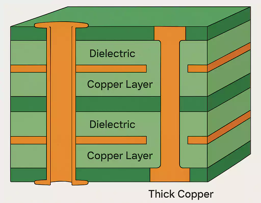
In power and motor-control applications, thick-copper PCBs (2 to 4 oz or more) are used to carry large currents and distribute heat efficiently. Designers often combine thick inner copper layers with heat-spreading vias and thermal relief pads to minimize hotspots.
The stackup—the arrangement of conductive and dielectric layers—directly affects impedance control, EMI performance, and thermal paths. Proper reference planes and balanced layer structures help reduce signal noise and mechanical warping.
Surface finishes also play a role in long-term reliability. ENIG (Electroless Nickel Immersion Gold) is preferred for its oxidation resistance and excellent solderability, while OSP and Immersion Silver offer cost-effective alternatives for less harsh environments.
End-to-End Manufacturing Process
Industrial PCB manufacturing follows the same general steps as standard PCB production, but with stricter controls and additional verification at each stage.
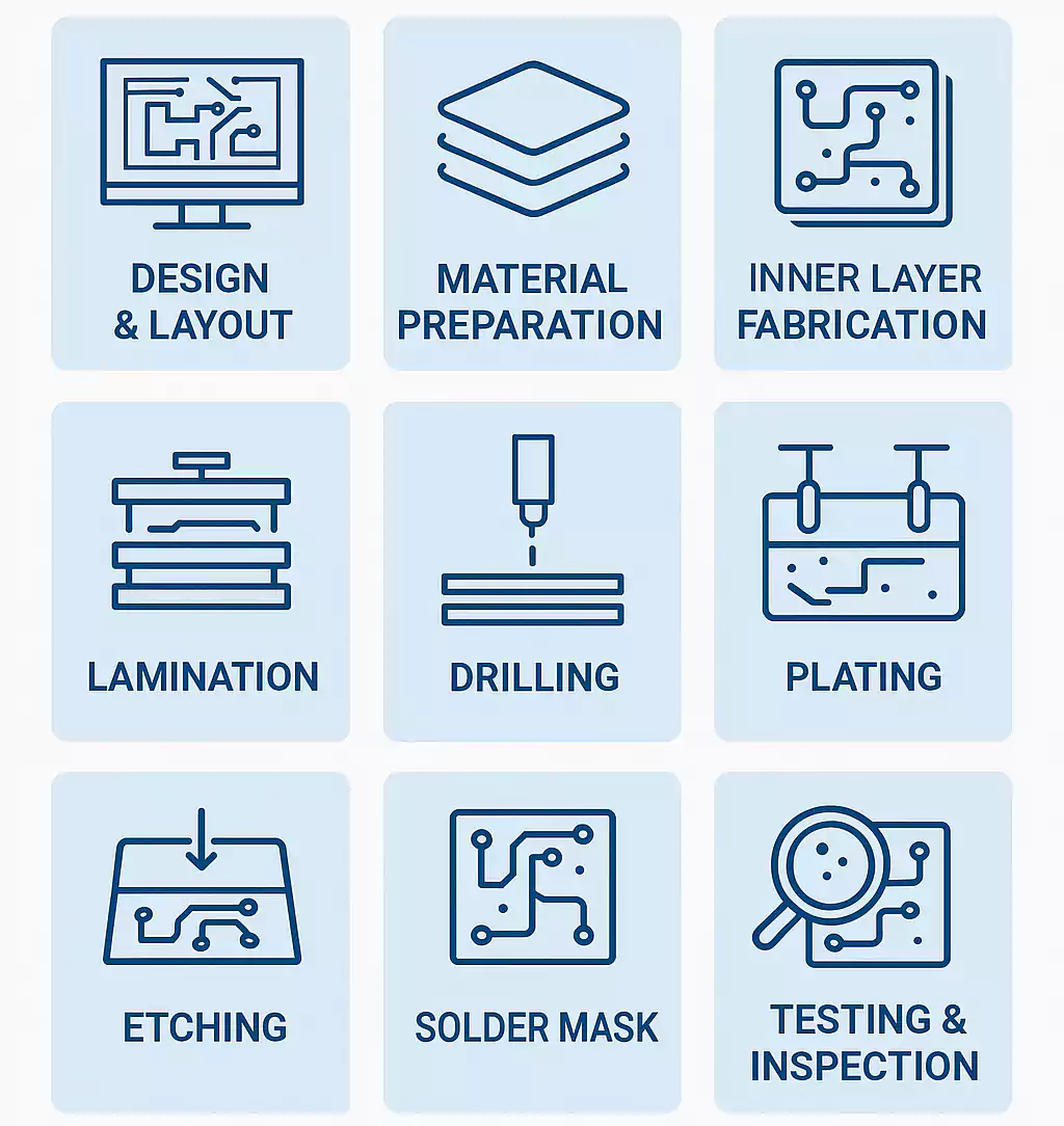
- Design and DFM Review – The process begins with a detailed Design for Manufacturability (DFM) review. Engineers verify clearances, copper balance, drill tolerances, impedance, and thermal management features to ensure the design meets industrial reliability standards.
- Inner Layer Fabrication – Copper foil is laminated onto dielectric cores and imaged with the circuit pattern. Etching removes unwanted copper, forming inner traces.
- Lamination and Layer Alignment – Multiple cores and prepreg sheets are stacked and pressed under heat and pressure to form a multilayer board. Alignment accuracy is crucial for maintaining signal integrity and ensuring drill precision.
- Drilling and Plating – Precision drilling creates via holes, which are then chemically cleaned and copper-plated to ensure solid electrical connections between layers. Industrial boards often require thicker copper plating (≥25 µm) for better current carrying and fatigue resistance.
- Outer Layer Imaging and Etching – The top and bottom circuits are patterned and etched to form traces. High-density or fine-pitch boards utilize advanced photolithography for precise tolerances.
- Solder Mask, Silkscreen, and Surface Finish – The solder mask protects copper traces from oxidation and short circuits. Industrial PCBs often utilize heat-resistant, chemically resistant mask formulations.
- Electrical Testing (E-Test) – 100% of industrial PCBs are tested for opens, shorts, and continuity. Flying-probe or fixture-based testers validate every net.
- Final Inspection and Packaging – Dimensional checks, solderability tests, and visual inspection under AOI verify the product meets IPC-6012 Class 2 or Class 3 requirements before shipping.
Quality Assurance and Reliability Testing
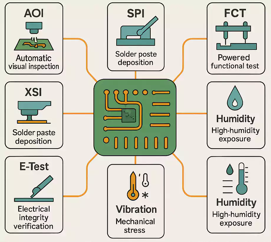
Quality assurance is the defining difference between industrial and consumer-grade PCB manufacturing. Beyond the standard electrical test, industrial PCBs undergo multiple inspections and reliability evaluations to ensure long-term stability.
- AOI (Automated Optical Inspection) detects micro-defects like nicks, shorts, and open traces early in the process.
- X-ray inspection examines plated-through holes, vias, and BGA solder joints for hidden defects.
- In-Circuit Testing (ICT) verifies component values, connections, and electrical performance after the component is assembled.
- Functional Testing (FCT) simulates real-world operation to validate board behavior under load.
- Environmental and Stress Tests, such as thermal cycling, vibration, humidity, and salt-spray aging, confirm mechanical and electrical durability.
DFM Tips for Industrial Designs
Designing for industrial PCB manufacturing requires thinking beyond connectivity—it’s about ensuring reliability under stress. Here are key DFM principles:
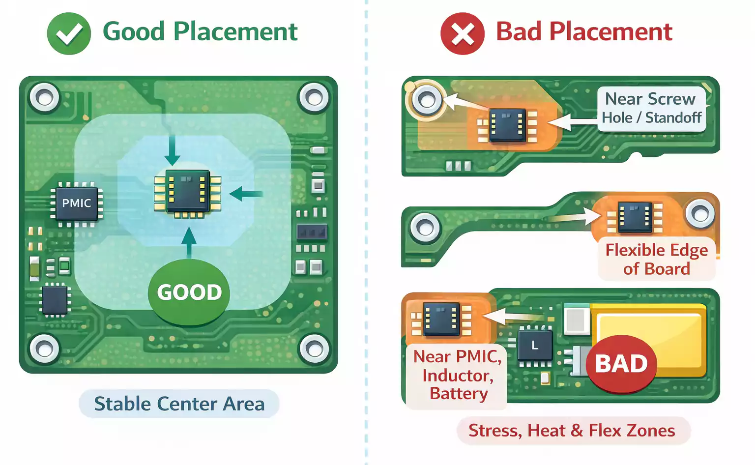
- Creepage and Clearance: Maintain sufficient spacing between conductive elements to prevent arcing under high voltage or high humidity conditions.
- Thermal Design: Utilize copper pours, thermal vias, and balanced copper distribution to efficiently dissipate heat.
- Via Reinforcement: For heavy components or high-current paths, use filled and plated vias (via-in-pad) to improve mechanical strength.
- Panelization: Plan for manufacturing yield—avoid fragile board outlines or sharp cutouts that may warp during lamination.
- Solder Mask Expansion: Adjust for manufacturing tolerances to prevent mask slivers or solder bridging.
Cost and Lead Time Factors
Industrial PCB projects typically cost more than consumer boards due to the use of higher-grade materials, thicker copper, additional testing, and tighter tolerances. However, understanding the key cost drivers helps optimize design without sacrificing reliability.
- Layer Count and Copper Weight: Increasing the number of layers and the weight of copper both increase material cost and processing complexity.
- Surface Finish: ENIG and Immersion Silver are pricier than OSP but offer better durability.
- Material Availability: Specialty laminates (polyimide, ceramic, or high-frequency substrates) may have longer procurement lead times.
- Testing Requirements: Full electrical and environmental testing adds cost but ensures consistent performance.
- Production Volume: Higher quantities lower per-unit cost, but industrial boards often run in smaller batches—requiring efficient setup and planning.
Typical lead times for industrial PCBs range from 10 to 20 working days, depending on the layer count, copper thickness, and complexity of the finishing process.
Industrial Applications
Industrial PCBs are used in nearly every sector that demands durability and precision. Common applications include:
- Factory Automation and PLCs: Require high signal integrity and noise immunity for control logic.
- Power Electronics and Inverters: Utilize thick-copper PCBs to handle large currents and dissipate heat effectively.
- Robotics and Sensors: Need flexible or rigid-flex designs that can withstand vibration and motion.
- Renewable Energy Systems (Solar, EV Chargers, BMS): Demand boards resistant to temperature swings and high voltage.
- Transportation and security systems require wide operating temperature ranges and long service life.
How to Choose an Industrial PCB Manufacturer
Selecting the right manufacturing partner can make or break your project. When evaluating suppliers, consider the following capabilities:
- Certification and Compliance: Look for certifications from IPC, UL, ISO, and IATF, which demonstrate adherence to global standards.
- Experience with Industrial and High-Reliability PCBs: A proven track record in thick-copper, HDI, or high-temperature boards ensures fewer process risks.
- DFM and Engineering Support: The best suppliers review your files and suggest design improvements before production.
- Testing and Inspection Capabilities: In-house AOI, X-Ray, ICT, and environmental chambers show a commitment to quality.
- Traceability Systems: Serial numbers and process data tracking are vital for industrial customers.
- Communication and Project Management: Timely updates, transparent pricing, and technical responsiveness build trust and efficiency.
At Fast Turn PCBs, we offer one-stop PCB fabrication and assembly under the same roof, helping streamline logistics, reduce lead times, and ensure greater control over quality from start to finish.
FAQs
1. What’s the main difference between industrial and consumer PCBs?
Industrial PCBs are designed for harsh environments, long life cycles, and continuous operation. They use higher-grade materials, thicker copper, and undergo more stringent testing.
2. When should I choose thick-copper or high-Tg materials?
Use thick copper (≥2 oz) for high-current circuits and high-Tg laminates for applications exceeding 130°C or involving repeated thermal cycling.
3. Which tests are mandatory for industrial PCBs?
At a minimum, electrical testing (E-Test) and AOI are standard. For critical systems, add X-Ray, ICT, and environmental stress testing.
4. How do I choose between ENIG and OSP surface finishes?
ENIG offers better oxidation resistance and is preferred for long-term storage or multiple reflow cycles. OSP is cheaper but best for short-term assembly.
Conclusion
Industrial PCB manufacturing is about far more than producing a functional circuit—it’s about ensuring longevity, consistency, and safety in demanding environments. Meeting international standards, selecting the right materials, and adhering to rigorous process control are key to achieving reliable performance.
By focusing on four pillars—standards compliance, reliability testing, DFM optimization, and supplier partnership—engineers can build industrial electronics that operate flawlessly for years. Whether you’re designing a new automation controller or upgrading a power management system, partnering with an experienced industrial PCB manufacturer will ensure your design performs as intended, even under the most challenging conditions.
