

Introduction
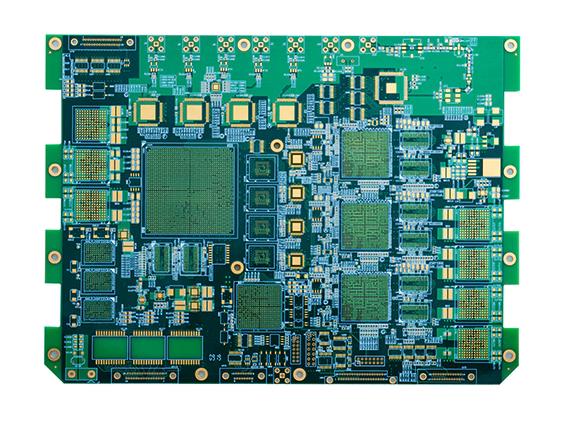
As packaging technologies such as BGA (Ball Grid Array) and CSP (Chip Scale Package) continue to advance, the demand for higher interconnect density in PCB assemblies continues to grow. The increase in PCB wiring density affects every component of the base material and its manufacturing process. To achieve reliable high-density interconnection (HDI), the component pitch must be reduced, which in turn requires tighter trace spacing and smaller plated-through holes.
Three Main Methods to Improve PCB Wiring Density
Generally, there are three ways to increase the wiring density of a PCB:
- Reduce conductor width and spacing.
- Add more circuit layers.
- Shrink via and pad dimensions.
Each approach comes with its own trade-offs among manufacturability, cost, and performance. Let’s explore each one.
1. Reducing Conductor Width and Spacing
The most direct way to pack more circuits into the same area is by reducing line width and spacing. Fine-line etching enables smaller traces and tighter routing, but it also narrows the fabrication process window.
To maintain good etching yield, manufacturers must use smooth copper foils with controlled surface roughness. A lower-roughness copper surface enables cleaner line definition, which is essential for 25 µm or even sub-25 µm line-space designs used in advanced HDI boards.
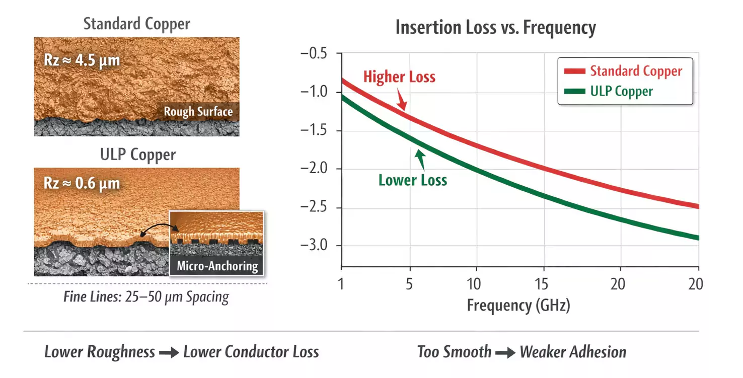
However, there’s a catch: smoother copper generally provides lower adhesion to the dielectric layer. The micro-rough peaks on traditional copper foil help resin anchor during lamination. Reducing those peaks weakens the bond strength, potentially leading to delamination or poor peel strength.
This creates a classic engineering trade-off:
| Fine-line etching | Low roughness (smooth) | Weaker adhesion |
| High peel strength | Higher roughness | Harder to etch fine lines |
In addition, surface roughness directly affects high-frequency electrical performance. At GHz frequencies, conductor loss increases with rougher copper because of the skin effect — current flows on the outer surface of the conductor. Rough copper increases the effective path length, causing higher insertion loss.
To address this, copper foil suppliers have developed ultra-low profile (ULP) and reverse-treated copper foils. These materials offer low roughness for minimal conductor loss and nano-anchoring treatments for enhanced adhesion, balancing signal integrity, etching precision, and lamination reliability.
2. Increasing the Number of PCB Layers
When horizontal space runs out, the next logical step is to add more layers. Multilayer PCBs allow designers to route more signals vertically by stacking multiple copper and dielectric layers.
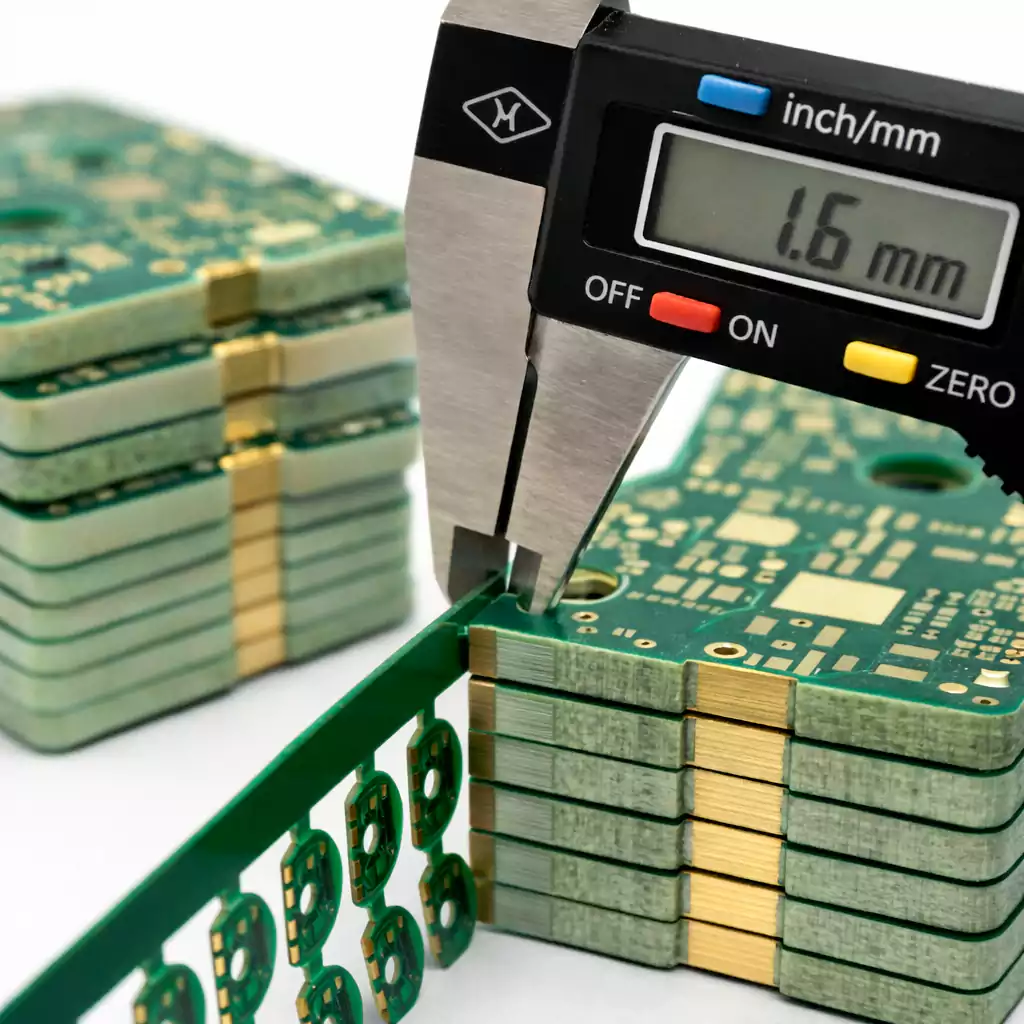
However, adding layers makes the board thicker overall, while each individual dielectric layer becomes thinner. This change introduces new challenges:
- Thickness control: Thinner dielectrics require tighter manufacturing tolerances to maintain consistent impedance and isolation.
- Thermal stability: A thicker stack-up retains more heat during lamination and reflow. Materials must withstand repeated thermal stress without warping.
- Registration accuracy: More layers increase the likelihood of misalignment during lamination. Even a 25 µm shift between layers can cause open or short circuits in fine-pitch HDI structures.
Registration (layer-to-layer alignment) depends heavily on the dimensional stability of laminate materials. The core and prepreg materials expand and shrink with heat and pressure. When thin cores are used to build high-layer-count boards, dimensional stability becomes harder to control, making precise alignment more difficult.
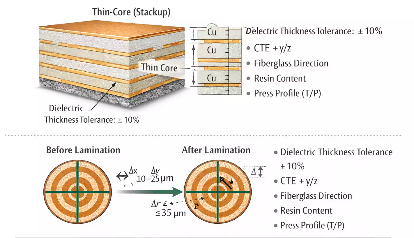
To maintain alignment yield, PCB manufacturers must manage:
- Lamination pressure and temperature profiles
- Glass cloth orientation and resin content
- Material coefficient of thermal expansion (CTE)
At FastTurn PCBs, our engineers use tight lamination control and X-ray alignment systems to achieve consistent registration accuracy across multilayer HDI stack-ups.
3. Shrinking Via and Pad Dimensions
Another effective way to increase wiring density is by reducing the size of vias and pads. Smaller vias open more routing channels between components and layers. This approach is fundamental to HDI (High-Density Interconnect) design.
Key technologies include:
- Laser-drilled microvias — typically 75 µm to 100 µm in diameter, connecting one or two adjacent layers.
- Via-in-pad (VIPPO) — placing vias directly on component pads to shorten routing paths and save space.
- Sequential lamination — building stacked or staggered microvias layer by layer to achieve complex interconnections.
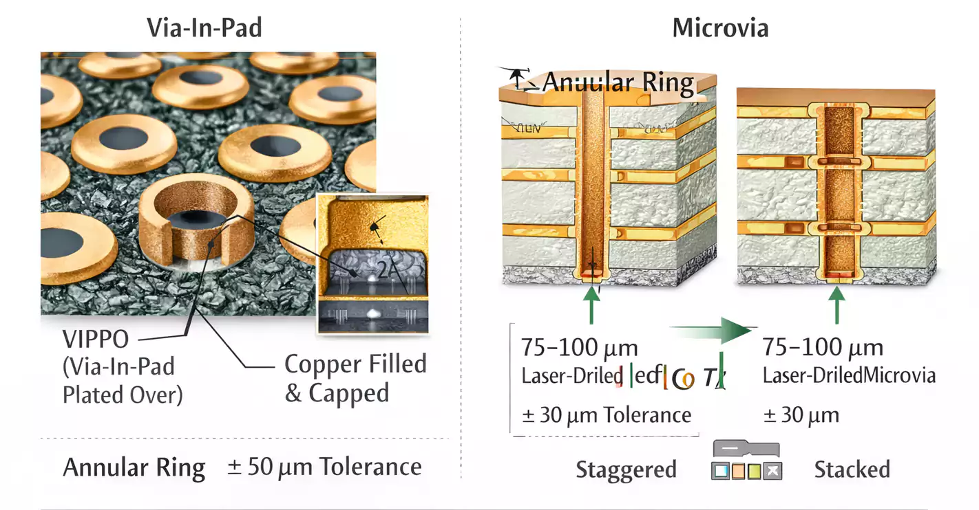
However, reducing the via and pad size also increases manufacturing difficulty. Smaller pads leave less annular ring tolerance, which demands better registration control and stable base materials. Poor dimensional stability can quickly lead to via breakout or misalignment, lowering yield.
Material suppliers like Isola and Panasonic emphasise dimensional stability as a key laminate property for advanced HDI designs. Using materials with low CTE and minimal resin shrinkage helps maintain high alignment yield during multilayer lamination and drilling.
Finding the Right Balance
To achieve better fine-line etching yield, manufacturers use low-roughness copper foil. But smoother copper also means weaker adhesion to the dielectric layer.
The challenge is to identify the optimal surface profile that maintains low roughness for fine-line etching and high-frequency performance, while still providing sufficient bond strength. Copper foil makers continue to develop new foil types that improve adhesion without increasing roughness.
Conclusion
The drive for higher circuit density continues to reshape the PCB industry. As packaging technologies evolve and operating frequencies rise, the need for fine-line capability, dimensional control, and low-loss materials will only grow stronger.
At FastTurn PCBs, we help customers navigate these challenges with:
- Advanced HDI stack-up designs
- Controlled-roughness copper options
- Precision lamination and registration processes
- Expertise in microvia and via-in-pad manufacturing
Whether you are developing compact consumer electronics or high-speed server boards, understanding how to balance copper roughness, layer count, and via design is key to achieving both performance and reliability.
