


Designing a printed circuit board (PCB) for the first time can seem complex. It involves art, science, and manufacturing disciplines. But once you grasp the workflow from schematic capture to final PCB artwork, the process becomes logical and organized.
This guide walks you through every major step of how to design PCB board, including schematic best practices, stack-up and impedance planning, layout and routing rules, and how to prepare files for manufacturing.
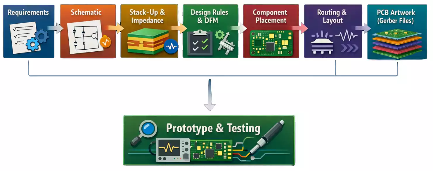
Step 1 — Define Design Requirements Before You Open CAD
Every great PCB design begins with clear requirements. Before you start drawing traces, spend time defining both electrical and mechanical constraints:
- Electrical: voltage rails, current load, signal types (analog, digital, high-speed), clock frequencies, impedance-sensitive nets, and interface standards (USB 3.0, PCIe, LVDS, etc.).
- Mechanical: board outline, height limits, mounting holes, connectors, and keep-out areas for enclosures.
- Environmental and compliance: operating temperature, EMI/EMC expectations, safety ratings, and regulatory needs such as FCC or CE.
Create a simple design brief listing each block of your circuit, required interfaces, and power budgets. This becomes your roadmap for the schematic and PCB layout that follows.
Step 2 — Draw the PCB Board Schematic (The Electrical Blueprint)
Your schematic defines how every component connects — it’s the logic behind your board. Poor schematic hygiene leads to layout chaos later, so apply a few essential practices:

Keep libraries clean and consistent
Use verified symbol and footprint libraries, or create your own. Ensure every schematic symbol maps to the correct PCB footprint and 3D model. Mismatched packages are one of the most common beginner mistakes.
Use clear naming and hierarchy
Name nets and signals meaningfully (USB_D+, ADC_IN1, 3V3_SYS). For larger projects, organize by hierarchical sheets — power supply, MCU, interface, sensors — so each function is self-contained and reusable.
Run ERC (Electrical Rule Check)
Before exporting to layout, run an ERC to detect floating pins, unconnected power nets, or multiple drivers on the same signal. Fixing them now saves rework later.
Manage your BOM early
Choose parts with a stable supply and check for alternatives. Nothing derails a design like an obsolete IC during production.
Step 3 — Plan the Stack-Up and Basic Impedance
Once your schematic is clean, open a blank PCB and define its stack-up. The stack-up is the arrangement of copper and dielectric layers. Stack-up affects impedance control, crosstalk, and manufacturability.
- 2-layer boards are common for simple analog or low-speed digital circuits.
- 4-layer boards (signal / ground / power / signal) are the sweet spot for mixed-signal and moderate-speed designs.
- 6-layer or more for high-speed interfaces or dense BGA components.

For impedance-controlled signals such as USB, Ethernet, or RF, communicate with your PCB manufacturer early. They’ll provide material data (dielectric constant Dk, thicknesses, and tolerances) so you can calculate trace width and spacing for 50 Ω single-ended or 100 Ω differential pairs.
A good stack-up ensures continuous ground planes under high-speed traces and minimizes return-path discontinuities — one of the biggest signal-integrity killers.
Step 4 — Set Design Rules and DFM Constraints Early
Before placing components, configure design rules (DRC) in your CAD tool.
| Minimum trace width / spacing | 5 mil / 5 mil |
| Minimum via drill / annular ring | 0.3 mm / 0.15 mm |
| Minimum solder mask bridge | 4 mil |
| Silkscreen text height | ≥ 40 mil |
| Copper thickness | 1 oz (35 µm) |
These parameters vary, so verify your fabricator’s capabilities before routing.
Good designers apply DFM (Design for Manufacturability) principles early — designing within realistic tolerances rather than pushing limits that raise costs or reduce yield.
Step 5 — Component Placement: Organize by Function
Placement defines not only the visual layout but also electrical performance, manufacturability, and serviceability.
- Group components by function. Keep power regulators, analog front-ends, and microcontrollers in their own zones.
- Follow signal flow. Inputs on one side, outputs on the other, so current and signal direction make sense.
- Minimize path length for high-speed, sensitive analog traces.
- Place decoupling capacitors as close as physically possible to IC power pins — with short, direct vias to the ground plane.
- Reserve mechanical keep-outs for connectors, heatsinks, and mounting holes.
- Leave accessible test points for probes and manufacturing test fixtures.
Think in terms of modular “islands” that simplify routing later.

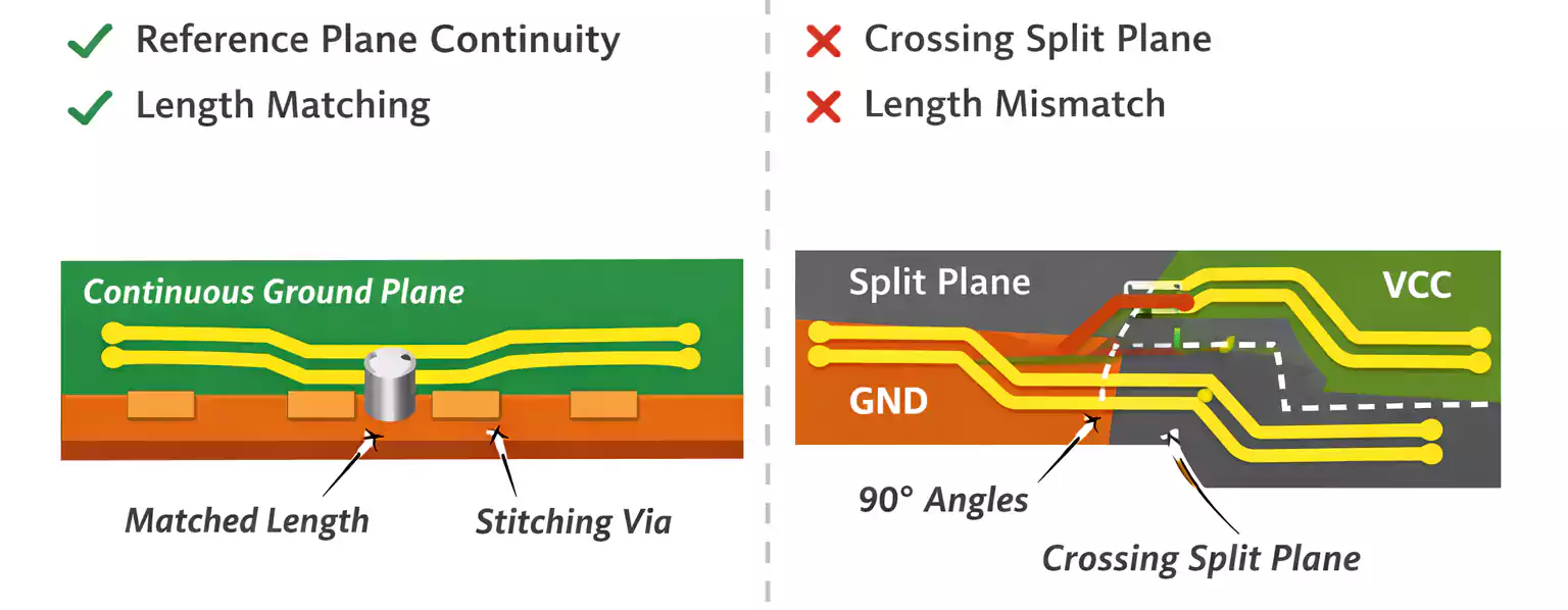
Step 6 — Vias, Planes, and Return Paths
Vias connect layers but also introduce inductance and potential signal reflections if misused.
- Through-hole vias are the cheapest and most common.
- Blind/buried vias save space in dense HDI designs but add cost.
- Always ensure there is a continuous return path under every signal. Do not route a high-speed trace across a split in the reference plane. This forces the current to detour, creating noise and EMI issues.
- When a signal changes layers, place a stitching via nearby to give the return current a short route back to ground.
For high-current paths, use multiple vias in parallel or filled vias to lower resistance and improve thermal dissipation.
Step 7 — Routing Strategy and Priorities
Routing is where the board truly takes shape. To avoid spaghetti chaos, route in order of importance:
- High-speed differential pairs (USB, HDMI, Ethernet). Keep lengths matched and maintain consistent spacing for impedance.
- Timing-critical signals (clocks, resets). Keep short and isolated.
- Sensitive analog traces (sensors, amplifiers). Separate from digital noise sources and, if needed, surround with guard rings.
- General digital signals. Use 45° angles instead of sharp 90° corners to maintain signal quality.
- Power traces and planes. Use wide copper pours to minimize IR drop and improve heat spreading.
When possible, route one layer horizontally and the next vertically to reduce crosstalk.
After routing, run DRC and inspect each net’s continuity and clearance.
Step 8 — Thermal, EMI/EMC, and Reliability Considerations
Even low-power boards generate heat and radiate EMI if not designed carefully.
Thermal management
- Use copper pours and thermal vias to spread heat from regulators, MOSFETs, or LEDs to larger copper areas.
- For components under heatsinks, ensure solder mask clearance for good thermal contact.
- Check that neighboring components won’t be overheated during reflow.
EMI/EMC basics
- Maintain continuous ground planes and avoid loops.
- Keep high-speed traces short and away from board edges.
- Place ferrite beads or common-mode chokes near I/O connectors.
- Add small RC filters to noisy lines if necessary.
Reliability
- Avoid vias in pads unless filled and plated.
- Use teardrops on critical traces for mechanical robustness.
- Verify manufacturability with IPC-A-600/610 class requirements if targeting industrial or automotive use.
Step 9 — From Layout to PCB Artwork
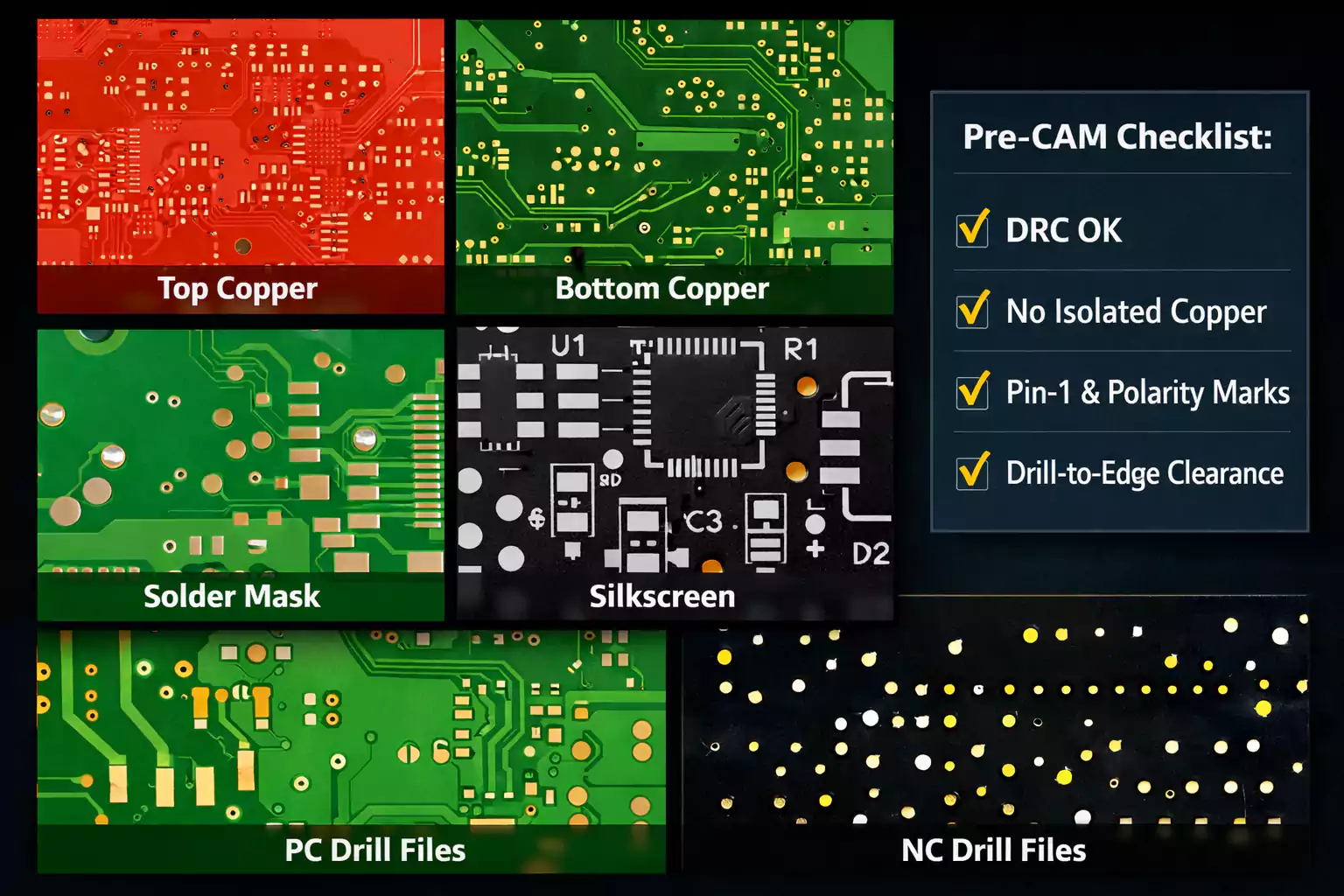
The term “PCB artwork” refers to the manufacturing data that describes every layer of your board. It’s what your fabricator uses to create photolithographic films or digital imaging files.
What to include in your PCB artwork package
- Gerber files for all copper, solder mask, and silkscreen layers.
- NC Drill files for plated and non-plated holes.
- Read-me or fabrication notes: material, stack-up, copper weight, controlled impedance, finish (ENIG, HASL), and solder mask color.
- Fabrication drawing (FAB) with board outline, hole chart, and tolerance notes.
- Assembly drawing (ASSY) showing reference designators and polarity marks.
- Pick-and-Place file for automated assembly.
- Bill of Materials (BOM) with part numbers and suppliers.
Pre-CAM checks before sending
- Run DRC and fix all violations.
- Check for unconnected nets, isolated copper areas, and missing reference marks.
- Verify drill-to-edge clearance and component orientation (Pin 1, polarity).
- Name layers clearly (e.g., TopCopper.GTL, BottomMask.GBS) to avoid confusion.
Good PCB artwork ensures your manufacturer builds exactly what you designed — no surprises, no costly respins.
Step 10 — Prototype, Test, and Iterate
Build a small prototype batch first and validate:
- Power-up test: confirm voltage rails and current draw.
- Functional test: exercise all I/O, sensors, and communication links.
- Thermal test: measure hot-spot temperatures under load.
- Signal-integrity checks: scope critical nets for ringing or jitter.
Record every finding and feed it back into a controlled revision. The best designers treat iteration as part of the process, not a failure.
When to Use PCB Layout Services
Sometimes outsourcing makes more sense than doing everything in-house. Consider professional PCB layout services if:
- Your design involves high-speed interfaces, RF, or HDI rigid-flex geometry.
- You face a tight deadline, and your internal team lacks bandwidth.
- You need manufacturing documentation (FAB, ASSY, pick-and-place) prepared to IPC standards.
- You require signal-integrity or power-integrity simulations beyond the capabilities of basic layout tools.
A reliable partner helps you go from concept to production faster, while ensuring compliance with your manufacturer’s design rules.
FAQs
1. What’s the difference between schematic and layout?
The schematic defines logical connections — how components are electrically linked.
The layout implements those connections physically with copper traces, vias, and planes on a board. You verify the schematic with ERC (Electrical Rule Check) and the layout with DRC (Design Rule Check).
2. What exactly is PCB artwork?
PCB artwork is the manufacturing data set — Gerber, NC drill, and fabrication drawings — used by a PCB house to create your board.
Modern alternatives like ODB++ or IPC-2581 combine all layers and metadata into a single standardized file, but Gerber remains the most widely supported format.
3. Which CAD software should beginners use?
- KiCad — free, open source, ideal for hobbyists and startups.
- Altium Designer — industry-standard for professional and multi-layer projects.
- EasyEDA — browser-based and integrated with online fab services.
Choose based on complexity, collaboration needs, and export compatibility.
Conclusion
Whether you're designing a simple two-layer Arduino-style board or a complex multi-layer RF system, these ten steps form the foundation of success. Mastering them ensures not just a board that powers on — but one that performs reliably, meets manufacturing standards, and scales seamlessly from prototype to production.
Great PCB engineers don’t just connect components — they engineer for performance, reliability, and repeatability. By following this structured approach, you’re not just designing a board. You’re building a process, a standard, and ultimately, better products.
