


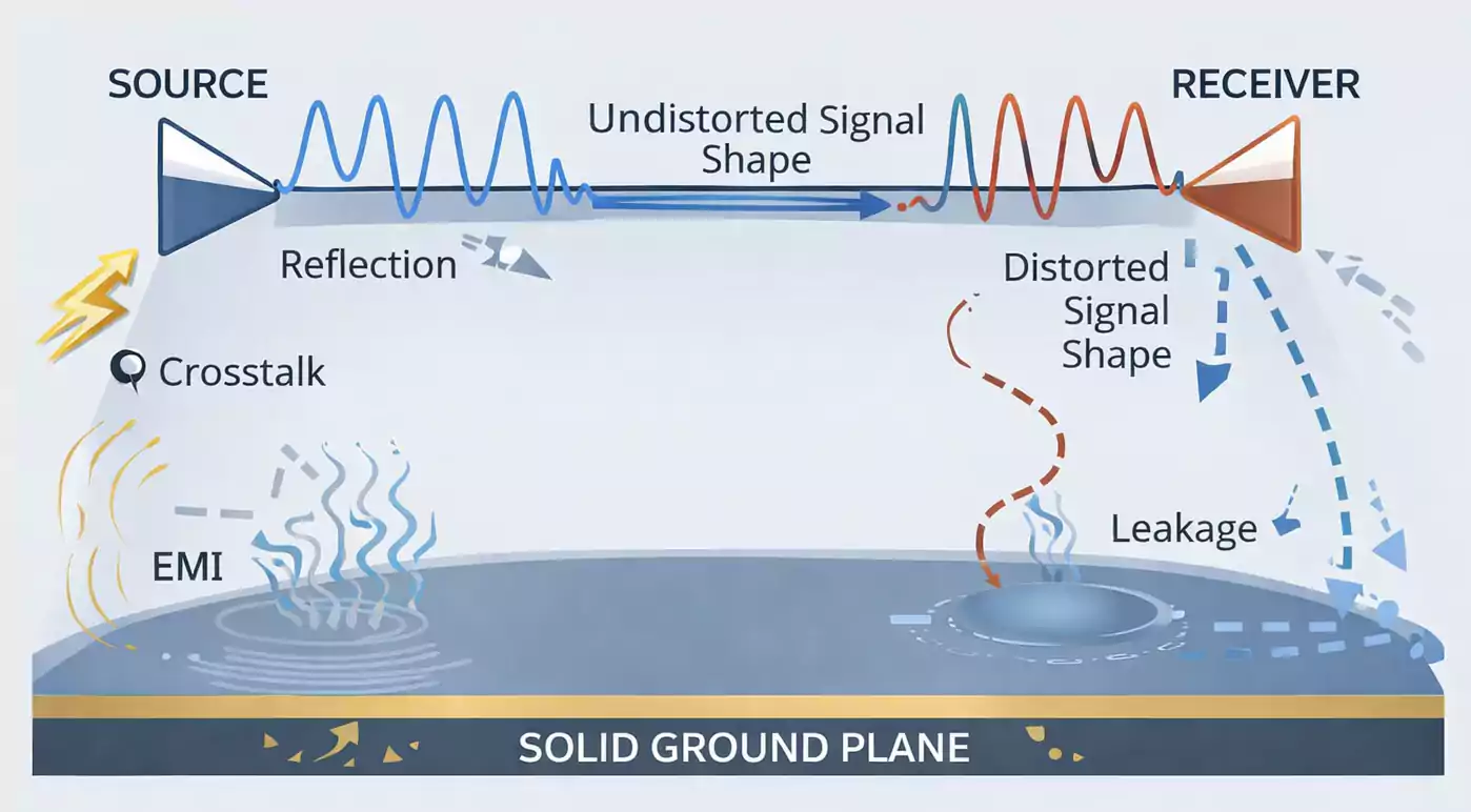
High-speed PCB signal integrity refers to a signal’s ability to maintain its intended waveform from source to receiver as frequency and data rate increase. If signal integrity is not properly controlled, issues such as reflection, crosstalk, EMI, ground bounce, and leakage can reduce performance and reliability.
For this reason, modern high-speed PCB design requires careful control of impedance, return paths, grounding, and layout. This is especially important in mixed-signal PCB design, where analog and digital circuits share the same board and can interact in complex ways.
This article outlines the main design challenges in high-speed systems, with a focus on leakage control and guard-ring layout for high-impedance inputs.
Why high-speed PCB design changes the rules
As switching speed and operating frequency increase, the PCB ceases to behave like a simple electrical connection platform. Layout choices that once seemed minor can now affect timing, waveform quality, noise, and emissions.
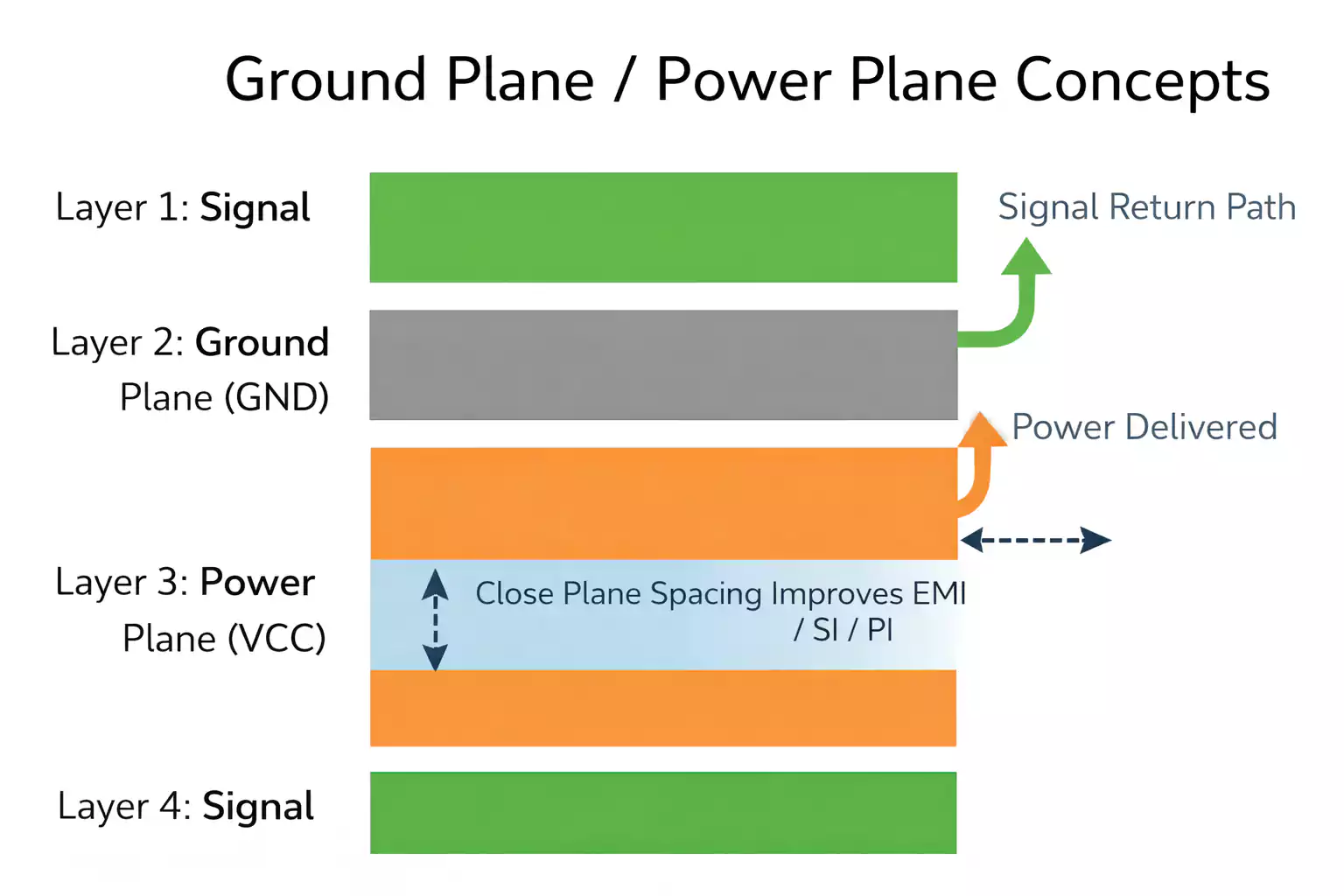
In low-speed designs, it is often possible to get acceptable results without paying close attention to return current paths, parasitics, or plane continuity. In a high-speed PCB, those details matter much more.
A few things start to dominate performance:
- routing style
- reference plane continuity
- return path quality
- stack-up structure
- package parasitics
- decoupling path inductance
At higher frequencies, digital design also starts to look a lot more like analog design. It is no longer enough to ask whether a logic level is technically correct. You also have to think about edge rates, coupling, impedance continuity, and how current actually flows through the board.
Another reason this gets harder is density. Modern systems pack more functionality into less space, and more of those devices use CMOS technologies. As frequency rises, power, heat, and switching noise typically become harder to manage.
Analog and digital are no longer cleanly separate
In older design workflows, analog and digital circuits were often treated as distinct worlds. In real high-speed systems, that separation is much less useful.
Fast digital edges contain significant high-frequency content. Because of that, digital circuits can run into problems often associated with analog or RF systems, including:
- reflections
- crosstalk
- uncontrolled return paths
- radiated emissions
- reference instability
At the same time, sensitive analog front ends often sit next to high-speed processors, clocks, or data interfaces on the same board. That means the analog and digital sections are not just neighbors. They interact.
This is why signal integrity and EMC are often addressed together. A routing problem may manifest as waveform distortion, but it can also cause emissions issues. Likewise, an apparent EMC problem may actually trace back to poor grounding, a broken return path, or an interrupted reference plane.
In mixed-signal PCB design, these issues are tightly connected.
Why leakage current matters more in modern boards
As supply voltages continue to fall, system noise margins also shrink. That makes even very small unwanted currents and voltages more important than they used to be.
In many circuits, PCB leakage current and leakage voltage are no longer negligible side effects. They can be close enough in magnitude to real signal levels that they begin to affect normal operation.
This becomes especially important in:
- sensor interfaces
- precision measurement systems
- low-level analog front ends
- high impedance input circuits
Even leakage in the nanoamp range, or a few millivolts of stray voltage, can introduce offset, reduce accuracy, distort a measurement, or destabilize a sensitive circuit.
Why high-impedance inputs are especially vulnerable
Low-level sensor systems are one of the most common places where leakage becomes a real design issue.
Sensors that measure temperature, pressure, strain, or force often generate very small electrical outputs. At the same time, those systems may be expected to deliver high accuracy. That combination creates a difficult condition: the signal is weak, but the performance target is strict.
To make those signals usable, the design usually includes signal conditioning and amplification stages. Those front ends often rely on high impedance input behavior to avoid loading the sensor.
That helps preserve the signal, but it also makes the input much more sensitive to:
- surface contamination
- humidity
- process residue
- stray voltage
- leakage paths
In other words, high input impedance improves measurement sensitivity, but it also raises sensitivity to unwanted interference.
Common sources of PCB leakage current
Leakage problems usually do not come from a single cause. They are often the result of interactions among materials, processing, contamination, and environmental conditions.
Common leakage sources
| Poor insulation performance | Reduces isolation between conductive regions |
| Flux or chemical residue | Creates weak conductive paths on the board surface |
| Fingerprints, oils, dust | Lowers surface resistance in sensitive areas |
| Humidity and moisture | Increases surface conductivity and leakage risk |
| Improperly cured materials | Leaves unstable or partially conductive residue |
| Contamination under coating or solder mask | Makes leakage harder to detect and harder to fix |
1. Inadequate insulation performance
If the substrate has weak surface insulation resistance or volume insulation resistance, unintended conductive paths can form more easily. In high-impedance circuits, even a small insulation failure can cause measurable errors.
2. Environmental and process contamination
Many leakage issues come from contamination rather than from the schematic itself. Common contributors include dust, fingerprints, skin oils, manufacturing residue, flux residue, and humidity-related moisture.
These contaminants reduce insulation performance and can create weak conductive paths in areas that should remain electrically isolated.
3. Surface and subsurface contamination
Not all contamination is visible. It may exist on the board surface, inside or around components, under the solder mask, or between a conformal coating and the surface it is supposed to protect.
That is one reason leakage issues can be difficult to diagnose. Visual inspection alone often is not enough.
The basic strategy: minimize potential differences
At the most fundamental level, leakage is driven by voltage difference.
If two nearby regions have significantly different potentials, unwanted current can flow between them. In practice, it is rarely possible to eliminate every potential difference in a real circuit, but it is often possible to reduce them around critical nodes.
A good leakage-control strategy usually includes three steps:
- Create a controlled protective region around sensitive conductors and input nodes.
- Keep unprotected conductors at different potentials away from high-impedance areas.
- Tie the protective structure to a low-impedance reference that closely tracks the protected node.
This approach reduces the voltage difference that drives stray current, making leakage much less likely to affect the circuit.
Guard rings: a practical way to control leakage
For sensitive analog inputs, a guard ring is one of the most useful PCB-level techniques available.
The basic idea is simple: place a conductive ring or guard trace around a high-impedance input region and hold that guard at a controlled potential. This helps reduce leakage caused by humidity, contamination, or surface conductivity near the input node.
What a guard ring does
A properly implemented guard ring can help:
- reduce surface leakage current
- protect sensitive input nodes
- improve stability in high-impedance circuits
- lower the effect of contamination and moisture
- support better measurement accuracy
Guarding is not just a layout trick
Good leakage control depends on more than trace geometry. It also involves:
- component selection
- package pin arrangement
- board material choice
- cleanliness and manufacturing control
Some components include unused or auxiliary pins near sensitive inputs. In some cases, those features can help improve isolation around the input region.
Adjacent pins can still be a problem
Nearby pins are not always electrically harmless. Inside the device, adjacent leads may connect to other amplifier stages or internal input structures. If those pins pick up leakage or coupling, they may still influence the protected input.
That is why guarding should be considered in the context of the full local input environment, not just a single pin.
Typical guard ring implementation
A common implementation is to place guard-ring traces around the sensitive input region on the relevant PCB layers and connect the guard ring to a low-impedance reference point.
Ideally, that reference follows the input signal voltage as closely as possible. In some analog applications, the recommended connection may instead be a designated shield node or enclosure-related reference, depending on the device and system architecture.
When the guard and the protected input are nearly at the same potential, the driving force for leakage current becomes much smaller. That is what makes guarding effective.
Quick design summary
Here is a simple way to think about the problem:
| High-speed digital routing | Signal degradation, EMI, return path issues | Control stack-up, routing, and reference continuity |
| Mixed-signal layout | Analog/digital coupling | Partition carefully and manage return currents |
| High-impedance inputs | Leakage and offset errors | Use guarding, spacing, and contamination control |
| Low-level sensor front ends | Weak signal corruption | Protect inputs early and minimize leakage paths |
| PCB cleanliness and materials | Surface conductivity | Improve process control, cleaning, and insulation quality |
Prevention works better than late fixes
Leakage control and signal integrity improvements are most effective when built in early.
Waiting until validation or troubleshooting to deal with these problems usually leads to more rework and less predictable results. A better approach is to treat leakage control, return path design, and input protection as front-end design decisions.
That is especially important in:
- precision analog circuits
- high-impedance input stages
- low-level sensor systems
- mixed-signal PCB design
- high-speed interfaces sharing the same board
In these designs, early choices about layout, material selection, process cleanliness, and protective structures often determine whether the finished product will be stable and accurate.
Conclusion
High-speed PCB signal integrity is not only about signal speed. The real issue is that parasitic effects, leakage, and return path discontinuities become much more significant as edge rates increase.
In this environment, signal integrity, EMC, grounding, and leakage control cannot be treated separately. They directly affect each other, especially in mixed-signal and high-impedance designs.
For that reason, effective high-speed PCB design depends on early control of layout, grounding, contamination, and input protection rather than late-stage correction. At FastTurnPCB, we value this design-first approach because it leads to more stable, manufacturable high-speed PCB solutions.
