In high-frequency PCB design, trace width is usually determined by impedance, not current capacity. For most RF and fast high-speed signals, the real question is not how much current a trace can carry, but whether it can maintain the target impedance—typically 50 ohms single-ended or 100 ohms differential.
That is why there is no universal “right” trace width for a high-frequency PCB. The correct width depends on the dielectric constant, substrate thickness, copper thickness, and transmission-line structure, such as microstrip or stripline.
A trace can be wide enough for current and still be electrically wrong for signal integrity.
Quick Answer
For high-frequency PCB design, trace width should not be chosen from a generic current table.
Instead, it should be calculated from:
- target impedance
- routing structure
- dielectric constant (Dk)
- dielectric thickness
- copper thickness
- nearby ground copper
- fabrication tolerance
That is why a 50-ohm trace width is never universal.
The correct width depends on the specific stackup and routing environment.
Why Trace Width Means Something Different in High-Frequency PCB Design
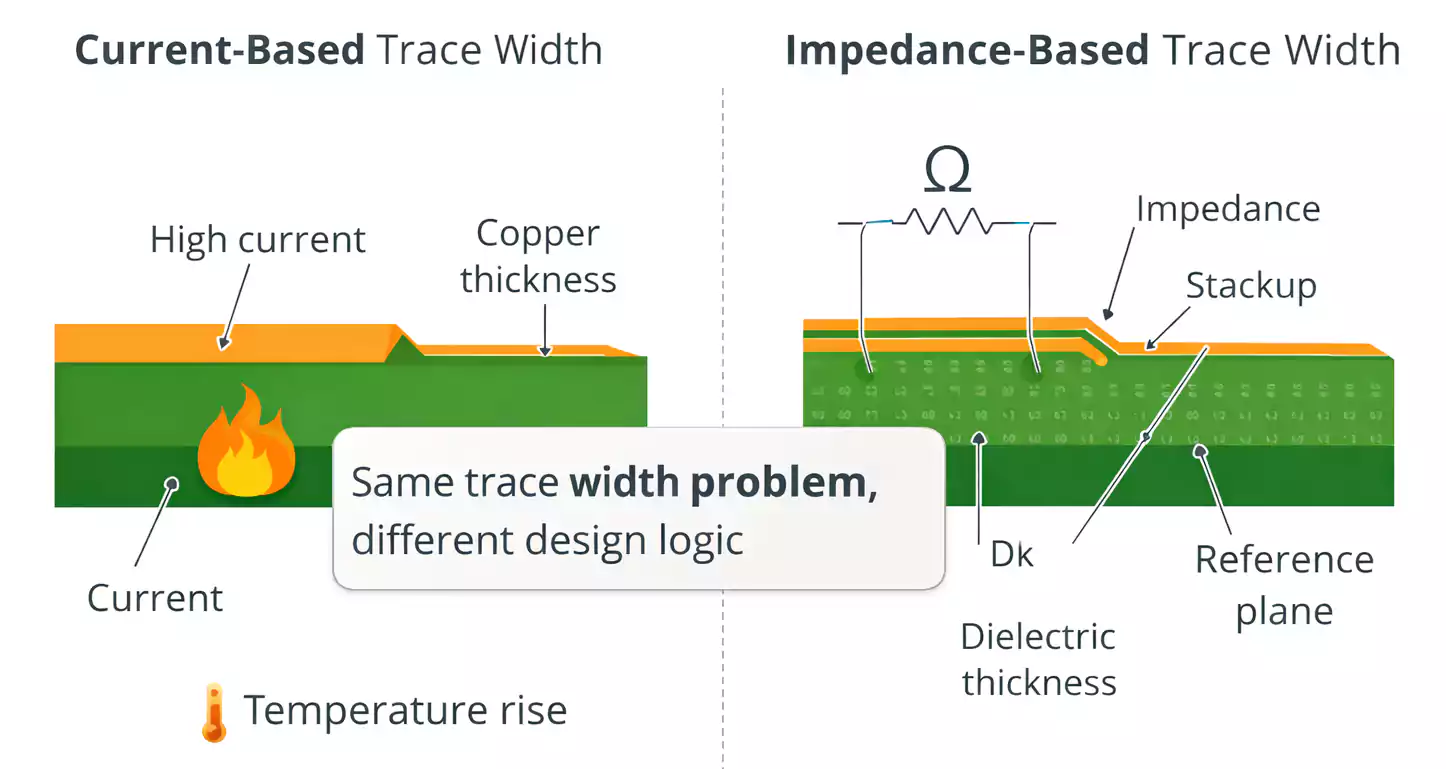
In low-frequency or power designs, trace width is usually chosen for one main reason: current capacity.
Designers want to make sure the copper does not overheat, especially on internal layers or high-current nets.
In high-frequency design, the problem changes.
A fast edge or RF signal does not behave like a simple DC current moving through copper. Once frequency rises and trace length becomes electrically significant, the trace behaves like a transmission line.
At that point, width is no longer just a mechanical or thermal choice. It becomes part of the impedance structure.
Current-Based Width vs Impedance-Based Width
| Current-carrying trace width | Current, copper thickness, allowable temperature rise, layer location | Power traces, supply rails, motor drive nets |
| Controlled-impedance trace width | Target impedance, stackup, Dk, dielectric thickness, copper thickness, routing geometry | RF traces, antennas, clock lines, fast digital nets |
This is where many PCB layouts go wrong.
A width that works perfectly for a power net may be a poor choice for a 50-ohm RF line. For a broader overview of PCB trace fundamentals, including current capacity, IPC-2152, and basic impedance considerations, see our PCB trace guide
When a PCB Trace Must Be Treated as a Transmission Line
Not every PCB trace needs controlled impedance.
But once signals become fast enough or frequencies are high enough, trace geometry starts to significantly affect signal behavior.
A trace should usually be treated as a transmission line when:
- The signal edge is fast.
- The route length is electrically long.
- The net is RF, microwave, or high-speed digital.
- reflections, ringing, or EMI matter
- Return path control is important.
In those cases, trace width must be selected as part of the transmission-line model, not from a rule-of-thumb current chart.
The Main Variables That Determine High-Frequency Trace Width
High-frequency trace width is not a standalone number. It is the result of several inputs working together.

1. Target Impedance
The most obvious input is the target impedance.
Common examples include:
- 50 ohm single-ended RF traces
- 75 ohm video or specialty lines
- 90 ohm differential pairs
- 100 ohm differential pairs
Different impedance targets require different geometries.
2. Transmission-Line Structure
The same trace width will not produce the same impedance in every structure.
The most common routing types are:
- Microstrip
- Stripline
- Coplanar Waveguide with Ground (CPWG)
Each one has a different field distribution, so each requires a different width to achieve the same impedance target.
3. Dielectric Thickness
The distance from the trace to its reference plane is one of the most important inputs in the calculation.
If that spacing changes, the impedance changes.
That means a width that works on one layer may be completely wrong on another layer.
4. Dielectric Constant (Dk)
The dielectric constant of the PCB material affects how signals propagate.
A trace routed on one laminate system may need a different width than the same trace routed on another material.
This is one reason why “50-ohm width” cannot be copied from board to board.
5. Copper Thickness
Copper thickness changes the effective conductor geometry.
It matters in both:
- current handling
- impedance calculation
A heavier copper trace does not behave exactly the same as a thinner one.
6. Nearby Ground Copper
This is often overlooked.
If ground copper is too close to a surface RF trace, the line may stop behaving like a simple microstrip and begin behaving more like CPWG.
That changes the impedance and can make the original width invalid.
7. Fabrication Tolerance
Even if the design width is correct in theory, the finished width after etching may vary slightly.
That is why practical impedance design must always include real-world manufacturing capabilities.
Choose the Routing Structure Before You Calculate Width
Before calculating the trace width, first define the transmission-line structure.
A 50-ohm trace does not have one fixed width. The required width depends on whether the line is routed as microstrip, stripline, or CPWG.
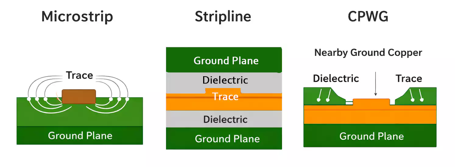
Microstrip
A microstrip is usually routed on the outer layer over one reference plane.
Advantages:
- easy to probe
- easy to tune during development
- Good for connectors and antenna feed lines
- simpler for short RF routes
Tradeoffs:
- more exposed to EMI
- more sensitive to nearby copper
- more influenced by the outside environment
Stripline
A stripline is routed on an inner layer between reference planes.
Advantages:
- better shielding
- lower radiation
- useful in dense multilayer designs
- better isolation in noisy environments
Tradeoffs:
- harder to probe and rework
- requires via transitions to reach surface components
- more dependent on stackup control
CPWG
A coplanar waveguide with ground uses a side-ground copper strip near the trace.
This can improve isolation and field control, but it also changes the impedance model.
That means you cannot calculate the trace as a normal microstrip and then add side ground later without recalculating it.
Why the Same “50 Ohm Width” Does Not Work Everywhere
This is one of the biggest misconceptions in PCB design.
A 50-ohm trace is not defined by width alone.
It is defined by width within a specific electrical environment.
That environment includes:
- the routing layer
- the reference plane
- dielectric thickness
- dielectric constant
- copper thickness
- nearby copper geometry
Change any of those, and the correct width changes too.
Example
A 50-ohm route may need:
- one width as an outer-layer microstrip
- a different width as an inner-layer stripline
- another width again if side ground is added for CPWG behavior
That is why copying a width from another board is risky, even if both boards are supposed to be “50 ohms.”
Step-by-Step: How to Calculate Trace Width for High-Frequency PCB Design
Here is a practical workflow that works much better than relying on generic charts.
Step 1: Start With the Stackup
Before calculating width, define:
- number of layers
- routing layer
- adjacent reference plane
- dielectric thickness
- copper thickness
Without a defined stackup, the width calculation is just a guess.
Step 2: Confirm Material Properties
Do not treat all laminates as identical.
For high-frequency designs, confirm:
- dielectric constant (Dk)
- loss tangent (Df)
- material family
- expected tolerance range
For RF boards, even a small material change can affect the final width.
Step 3: Choose the Trace Structure
Decide whether the route is:
- microstrip
- stripline
- CPWG
This decision comes before the width calculation, not after it.
Step 4: Run a First-Pass Impedance Calculation
Use an impedance calculator or field-solver-based tool to get an initial width estimate.
This first pass is useful for comparing options such as:
- outer-layer vs inner-layer routing
- thinner vs thicker dielectric
- standard vs low-loss material
- microstrip vs stripline
Step 5: Check Manufacturability
Now ask practical questions:
- Is the trace too narrow for stable production?
- Is the spacing realistic?
- Will etch compensation affect the final result?
- Can the fabricator hold the required tolerance?
An electrically correct geometry is not enough if it is difficult to manufacture consistently.
Step 6: Refine the Model for Higher Frequencies
At higher frequencies, the simplified model may not be enough.
Additional effects may matter more, including:
- copper roughness
- loss tangent
- conductor profile
- plating effects
- fabrication tolerance
The higher the frequency and the tighter the loss budget, the more important those details become.
A Simple Comparison: What Changes Trace Width?
| Higher target impedance | Required width usually gets narrower |
| Lower target impedance | Required width usually gets wider |
| Greater dielectric thickness | Required width usually changes significantly |
| Higher Dk | Width for the same impedance often changes |
| Thicker copper | Effective geometry changes |
| Move from microstrip to stripline | Width usually must be recalculated |
| Add nearby side ground | Microstrip behavior may shift toward CPWG |
This table is not a substitute for calculation, but it shows why width is always context-dependent.
Ground Clearance, Return Paths, and Crosstalk Still Matter
Getting the width right does not guarantee good RF performance.
The surrounding layout still matters.
Ground Clearance
If the side ground copper is too close to a surface trace, the impedance changes.
This is especially important for RF traces routed on outer layers.
A trace that was designed as a simple microstrip may no longer behave like one after nearby copper is added.
Return Path Continuity
High-frequency current needs a clean return path.
If the reference plane is split, interrupted, or poorly connected, signal quality can degrade even when the trace width is correct.
Crosstalk Spacing
Adjacent traces can couple energy between themselves.
Basic layout habits still matter:
- Keep enough spacing between sensitive nets.
- Reduce long parallel runs.
- avoid unnecessary coupling on RF layers
A properly calculated width cannot fix a layout that is noisy or poorly isolated.
Vias and Layer Changes Can Undo Good Trace-Width Design
Even with a perfect trace width, performance can still suffer if the signal path includes too many discontinuities.
Why Vias Matter
Vias introduce:
- parasitic inductance
- parasitic capacitance
- impedance discontinuities
- possible via stub effects
That is why high-frequency routes should usually use as few vias as possible.
Why Layer Transitions Matter
When a signal changes layers:
- The field structure may change.
- The reference environment may change.
- The impedance may change.
- The return path must be preserved.
A correct trace width on one layer does not automatically carry over to the next layer.
Common Mistakes in High-Frequency Trace Width Design
These mistakes keep showing up in real PCB layouts.
1. Using Current Tables for RF Traces
A power-trace chart is useful for thermal design.
It is not a valid substitute for impedance calculation.
2. Reusing the Same Width on Different Layers
Changing layers changes the dielectric spacing and reference environment.
That means the width often has to change, too.
3. Ignoring Nearby Ground Copper
A nearby ground pour can alter the field distribution and invalidate the original width.
4. Treating “FR-4” as a Precise Electrical Number
Material properties vary. High-frequency designs should not assume every laminate behaves the same way.
5. Forgetting Manufacturing Tolerance
A design width is not always the exact finished width after etching.
6. Focusing Only on Width
Width is important, but so are:
- return paths
- vias
- spacing
- transitions
- overall routing structure
A trace can be “correct” on paper and still perform poorly in the real board.
FAQ
What is the trace width for a 50-ohm microstrip?
There is no universal answer. It depends on the stackup, dielectric thickness, dielectric constant, copper thickness, and nearby copper.
Is a 50-ohm trace width the same on every PCB?
No. A 50-ohm width on one board may be wrong on another board with a different stackup or material.
Does copper thickness affect impedance?
Yes. Copper thickness changes the conductor geometry and can affect the final impedance result.
Is stripline wider or narrower than microstrip for the same impedance?
It depends on the stackup. The key point is that the two should not be assumed to use the same width.
Does nearby ground copper affect a microstrip?
Yes. If ground copper is close enough, it can change the field distribution and push the line toward CPWG behavior.
Can I use a current-based trace chart for RF layout?
No. Current charts are for thermal and current-carrying design, not controlled-impedance routing.
Final Thoughts
In high-frequency PCB design, trace width is a stackup-defined impedance parameter, not a standalone number. The right process is to define the structure, confirm the material, calculate the width, and verify manufacturability. For production builds, FastTurnPCB supports custom high-frequency PCB manufacturing while accounting for real-world stackup and fabrication requirements.