


When electronic signals reach gigahertz speeds, every millimeter of copper matters.
High-frequency PCBs are purpose-built to handle those signals with minimal loss, stable impedance, and reliable manufacturability.
If you are designing a 5G transceiver, radar front-end, or satellite module, this guide covers materials, stackups, layout rules, and collaboration with High Frequency PCB manufacturer to achieve first-pass design success.
What Is a High Frequency PCB?
A High Frequency PCB—sometimes called an RF or Microwave PCB—is designed for circuits that operate above 1 GHz (some industries draw the line at 500 MHz).
These boards use dielectric materials with low loss and stable electrical characteristics to control signal attenuation, crosstalk, and impedance drift.
Typical applications include:
- 5 G base stations and microwave backhaul links
- 24 GHz / 77 GHz automotive radar
- GPS and satellite communications
- Medical imaging and RF therapy systems
- Aerospace and defense telemetry
At these frequencies, the PCB substrate becomes part of the circuit itself. Dielectric constant (Dk), dissipation factor (Df), and even moisture absorption determine how your signals behave—so material selection and stackup are the foundation of every successful design.
Key Material Choices: Performance Starts with Dk and Df
1. Focus on Two Numbers — Dk and Df
- The dielectric constant (Dk) controls impedance, signal velocity, and the degree of coupling between traces.
- The Dissipation Factor (Df) directly determines insertion loss.
- Low water absorption helps maintain consistent Dk/Df under humidity or temperature swings.
Among the most widely used materials are Rogers RO4003C, RO4350B, and RO3003, which offer Dk values of 3.0–3.5 and Df as low as 0.001. These substrates combine excellent high-frequency performance with processability close to FR-4.
For even lower loss or higher power handling, many engineers turn to PTFE-based laminates from Taconic, Isola, Panasonic Megtron, or Arlon.
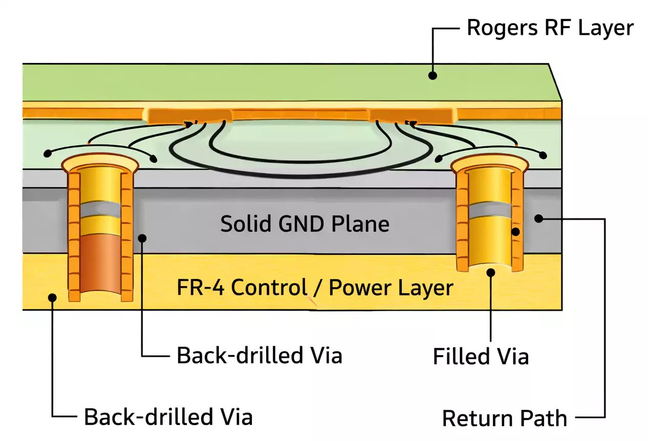
2. Rogers vs FR-4: Why Many Designs Use Hybrid Stackups
Pure Rogers/PTFE builds deliver the best RF performance, but they’re more expensive and mechanically softer than FR-4.
That’s why most production teams choose a Hybrid stackup:
- Rogers/PTFE for RF, antenna, and high-speed signal layers
- FR-4 for control logic, power, and mechanical stiffness
To make this work reliably:
- Keep the stackup symmetrical (equal copper on both sides) to avoid warpage.
- Control resin flow during lamination to prevent voids.
- Align copper thickness and impedance targets across materials to keep the final tolerance within ±5%.
At Fast Turn PCB, we routinely build Hybrid Rogers/FR-4 constructions with impedance control, back-drilling, and via filling.
Prototypes are available in 24–72 hours with MOQ = 1, allowing quick RF validation without long lead times.
3. Two Proven Stackup Models
- Single-Material RF Stackup:
Alternate Signal–Ground–Signal–Ground layers for predictable impedance. Place TDR coupons on the panel edge to verify trace geometry. - Hybrid Stackup:
Top RF layers and antennas on Rogers; control and power layers on FR-4 beneath.
Maintain mirror symmetry, use back-drill to remove via stubs, and keep critical traces above continuous reference planes.
our engineering team can share recommended Hybrid stackup templates for Rogers 4350B + FR-4 and 4003C + FR-4 combinations.
Design Rules: Turning Simulation into Manufacturable Reality
High Frequency PCB design isn’t only about equations—it’s about making the simulated model buildable.
Below are the practical layout and DFM principles that ensure your design performs the same on the bench as it does in the simulator.
1. Impedance Control — Target ±5 %
- Use microstrip or stripline geometries with well-defined dielectric height and copper thickness.
- Maintain a continuous reference plane under every critical signal; never route high-speed traces across plane splits.
- Include TDR test coupons for every controlled-impedance net. Correlate them with S-parameter measurements during validation.
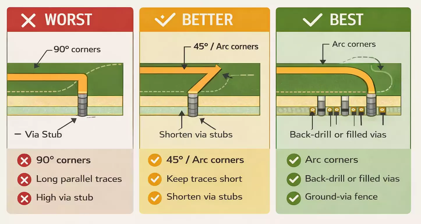
2. Routing, Corners, and Vias
- Keep traces as short as possible and minimize parallel runs.
- Replace sharp 90° corners with 45° bends or arcs to reduce reflection.
- Limit vias. Each via adds parasitic inductance and reflection; where unavoidable, use back-drilling, filled vias, or blind microvias.
- Maintain symmetry for differential pairs, matching both length and via transitions.
3. Crosstalk & EMI Basics
- Increase spacing between adjacent high-frequency lines.
- Route orthogonally between layers to minimize coupling.
- Add ground vias (fencing) along sensitive edges to form isolation walls.
- Separate high-current digital or power paths from high-Q RF sections.
4. Assembly Considerations
PTFE and hybrid materials expand differently during reflow. Confirm the reflow temperature profile and consider fixture or pin tooling for dimensional control.
Fast Turn PCB provides free DFM/DFT reviews and optional functional testing (FCT) before mass production—catching issues like bow, twist, or skew before they reach your line.
Typical High-Frequency Applications
While the physics are universal, design priorities differ by industry:
| 5 G / Telecom | 1–30 GHz | Power amplifiers, filters, antennas |
| Automotive Radar | 24 / 77 GHz | Short-range radar, ADAS |
| Satellite / GNSS | 1.5–12 GHz | Navigation, telemetry, up/down-conversion |
| Medical & Imaging | 1–10 GHz | MRI, RF ablation, diagnostic sensors |
| Aerospace / Defense | 2–40 GHz | Phased-array radar, avionics links |
Common Pitfalls and How to Fix Them
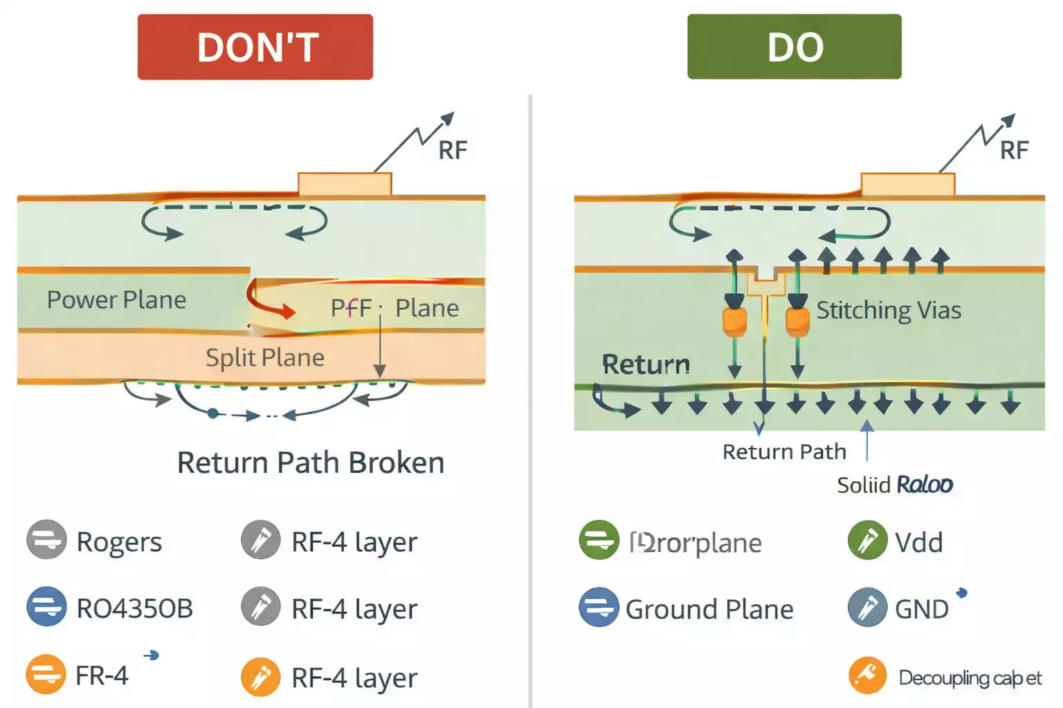
1. Broken Return Path
Critical nets routed across split ground planes lose their return path and radiate.
→ Keep RF traces above solid ground and bridge gaps with stitching vias.
2. Impedance Mismatch / Reflection
Variations in stackup, copper thickness, or trace width can swing impedance.
→ Lock stackup early, specify ±5 % tolerance, and validate with TDR coupons.
3. Excessive Vias or Long Stubs
Every via adds inductance; un-drilled stubs create resonances.
→ Back-drill or fill non-functional vias, and pair differential vias symmetrically.
4. Crosstalk or EMI Failures
Parallel routes, tight spacing, or missing ground fences can cause emissions to blow.
→ Increase spacing, add orthogonal routing, and use ground fencing.
5. Unapproved Material Substitution
Switching laminate suppliers mid-run changes Dk/Df and shifts impedance.
→ Maintain an approved material substitution matrix and validate alternatives with prototypes first.
Fast Turn PCB Capabilities at a Glance
- Material portfolio: Rogers 4350B/4003C/3003, Taconic RF-35/TLY-5, Isola, Panasonic Megtron, PTFE / ceramic-filled laminates
- Quick-turn options: 24 – 72 hour prototypes, MOQ = 1
- Engineering support: Free DFM/DFT review, impedance modeling, stackup consultation
- Manufacturing features: Impedance control (±5 %), back-drilling, via filling, blind/buried microvias, laser drilling, solder mask alignment within ±2 mil
- Assembly & testing: SMT down to 01005 components, fine-pitch BGA/QFN, optional FCT, and functional validation
With all services under one roof, you avoid the communication gap between fabrication and assembly—critical when dealing with expensive RF materials.
Frequently Asked Questions
Q1: Is “high frequency” defined as 1 GHz or 500 MHz?
Both thresholds appear in industry literature. For RF and microwave circuits, ≥1 GHz is the practical boundary. For high-speed digital buses, you may hit “RF-like” issues as low as 500 MHz—so the key is whether transmission-line behavior dominates.
Q2: When should I use a Rogers + FR-4 Hybrid?
Whenever you need high-frequency performance but can’t justify a full PTFE build.
Use Rogers/PTFE on critical RF layers and FR-4 elsewhere, keeping the stackup symmetrical and copper thickness matched.
Q3: How can I quickly reduce RF crosstalk?
Increase spacing, route differential pairs orthogonally between layers, and add ground via fences around sensitive regions. Even simple spacing adjustments can yield an improvement of> 10 dB.
Q4: Why does my measured loss exceed the simulation?
Common causes include copper roughness, slight trace-width error, long via stubs, incomplete ground return, or batch-to-batch Dk variation.
Ready to Build Your RF or Microwave Board?
Whether you’re prototyping a 5 G module or ramping to volume, success depends on working with a manufacturer who truly understands high-frequency materials and DFM trade-offs.
Fast Turn PCB provides end-to-end Microwave PCB Fabrication Service with:
- Rogers, Taconic, Isola, and PTFE material options
- Hybrid lamination and impedance-controlled builds
- Back-drill, via fill, blind/buried microvias
- 24–72 hour prototypes and flexible production volumes
- Direct engineer-to-engineer communication
Get a quote or upload your Gerber files today to connect with our High Frequency PCB Manufacturer team.
Need specific materials or stackup guidance?
