


When your design needs to handle high current, high temperature, or harsh environments, standard 1-oz copper is no longer enough.
That’s where Heavy Copper PCB, also called Thick Copper PCB, comes in.
With copper thicknesses ranging from 2 oz up to 20 oz and beyond, these boards can safely carry large currents, dissipate heat efficiently, and provide mechanical robustness that standard multilayer PCBs simply cannot achieve.
What Is a Heavy or Thick Copper PCB?
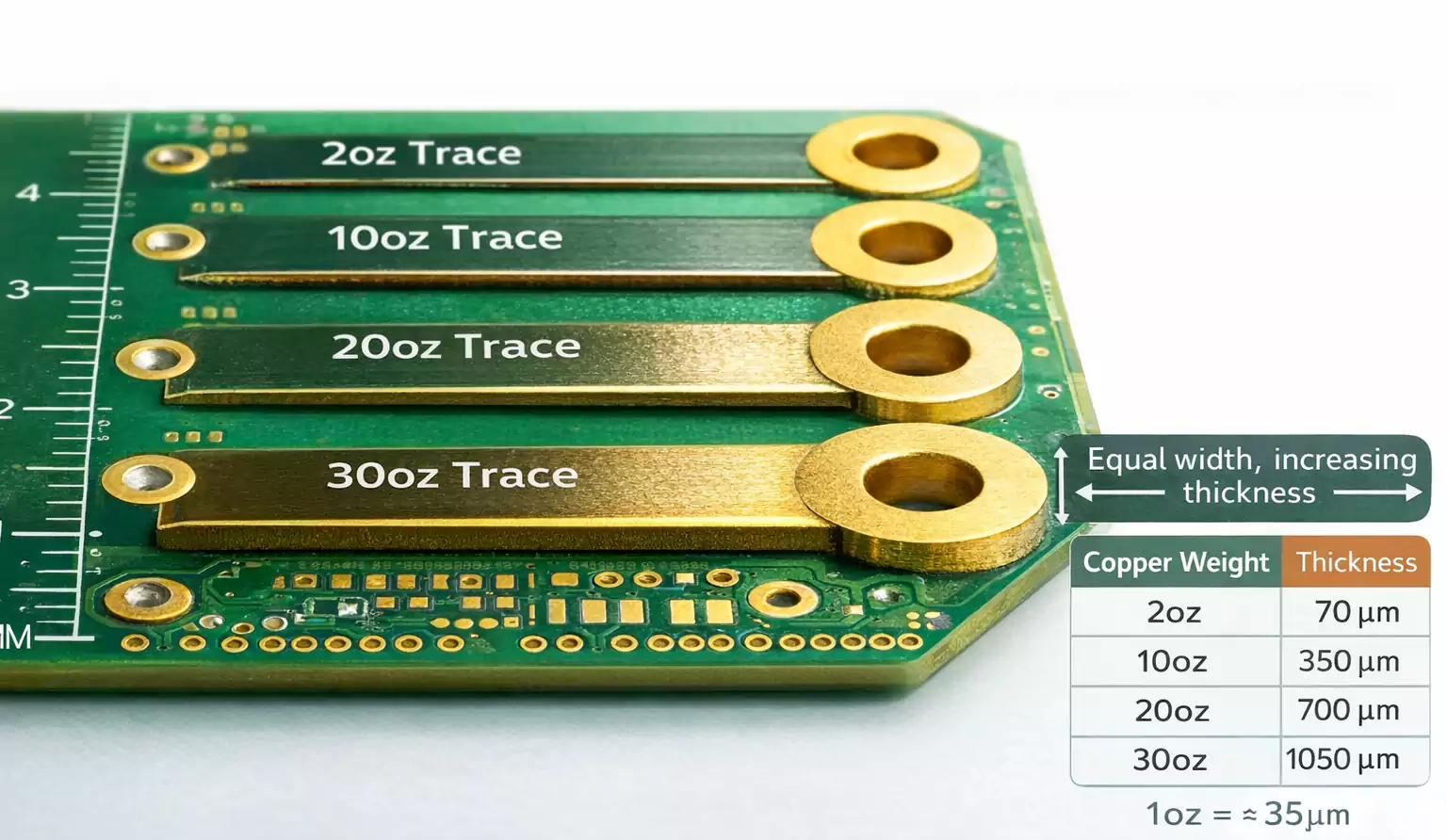
In the printed circuit industry, any layer with ≥ 2 oz of copper (≈ 70 µm) is generally considered a thick copper layer.
Standard PCBs use 1 oz (≈ 35 µm) copper, while heavy copper designs use 2–6 oz, and ultra-heavy versions reach 20 oz (≈ 700 µm) per layer or more.
Thick copper conductors are plated or laminated onto the substrate and then etched to form traces, pads, and planes.
Compared to standard boards, they offer:
- Higher current-carrying capacity
- Better heat conduction and distribution
- Stronger mechanical integrity in connectors and vias
- Improved reliability under thermal cycling
Why Engineers Choose Heavy Copper PCBs
1. High-Current Capability
The most obvious reason to use thick copper is current.
A wider and thicker copper trace has a larger cross-sectional area, reducing resistance (I²R loss) and limiting temperature rise.
That’s crucial in power converters, battery packs, and motor controllers where currents can reach tens or even hundreds of amps.
2. Superior Heat Dissipation
Copper’s thermal conductivity is roughly 400 W/m·K—hundreds of times higher than that of typical FR-4 epoxy.
A heavy copper PCB spreads heat more evenly across the board and into thermal vias or heatsinks, preventing local hotspots and extending component life.
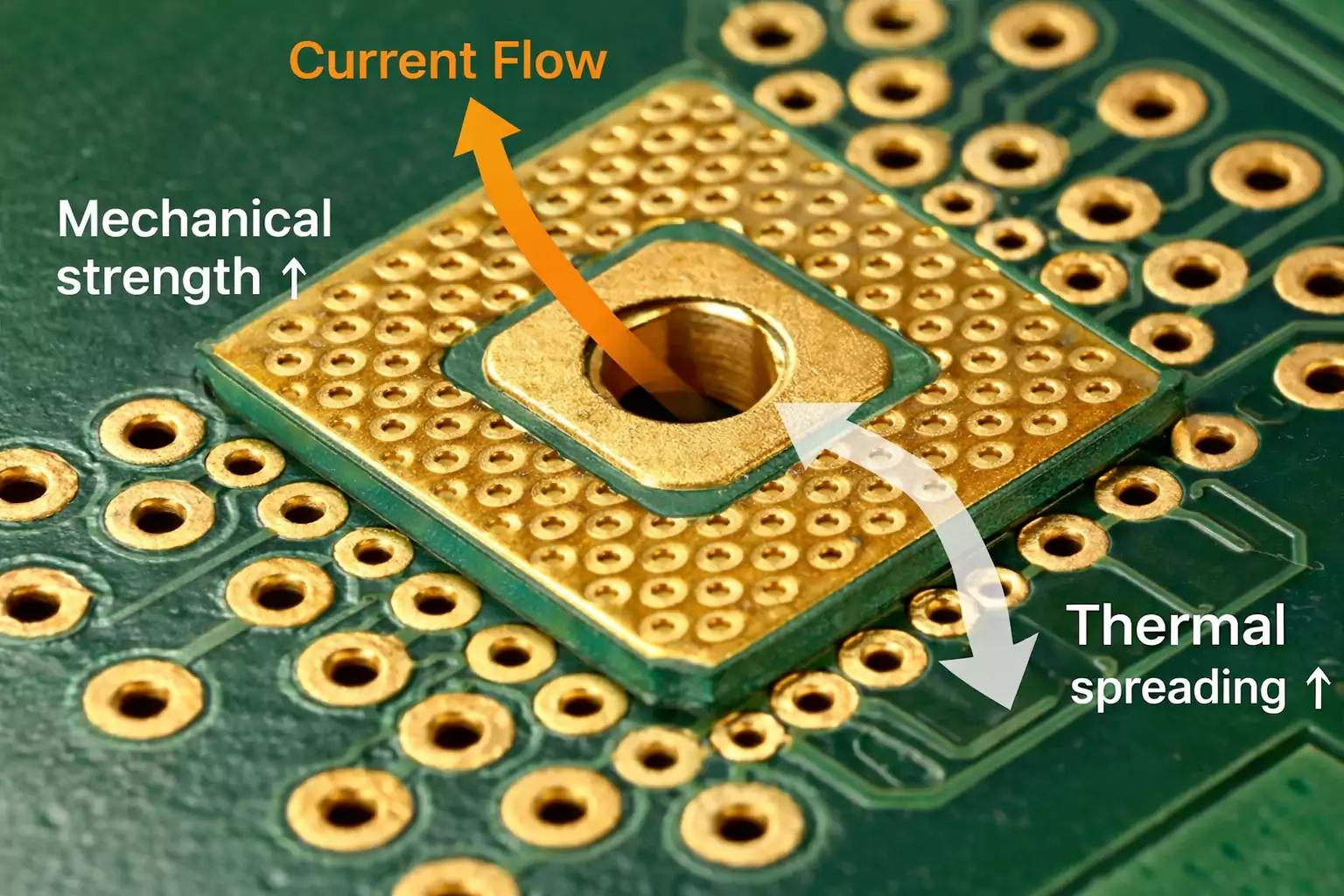
3. Mechanical Strength and Reliability
Thicker copper layers reinforce pads, vias, and terminal areas, making them more resistant to vibration, flexing, and thermal stress.
That extra durability matters for automotive, aerospace, and defense electronics, where mechanical shocks and wide temperature swings are the norm.
4. Power and Control on One Board
Heavy copper allows engineers to integrate power circuitry and control logic on the same PCB, rather than separating them into separate modules.
This reduces system size, interconnect losses, and assembly costs.
Copper Weight and Thickness Conversion
Designers often see copper specified in ounces per square foot (oz/ft²), which measures how much copper covers one square foot of the PCB laminate.
Here’s a quick reference:
| 1 oz | 35 µm | Standard signal layers |
| 2 oz | 70 µm | Moderate-current power rails |
| 3–4 oz | 105–140 µm | High-current applications |
| 6–10 oz | 210–350 µm | Power distribution, bus bars |
| 12–20 oz | 420–700 µm | Ultra-heavy copper, custom builds |
In real manufacturing, the finished copper thickness equals the base copper thickness plus the plated copper added during processing.
Fast Turn PCB routinely fabricates copper weights from 2 oz to 20 oz+ per layer, depending on the design.
Current-Carrying and Temperature Rise
The relationship between current, copper thickness, and temperature rise is one of the most important design considerations.
Current causes heat generation (P = I²R). The trace width and copper thickness determine the resistance, while airflow and board material determine how quickly heat dissipates.
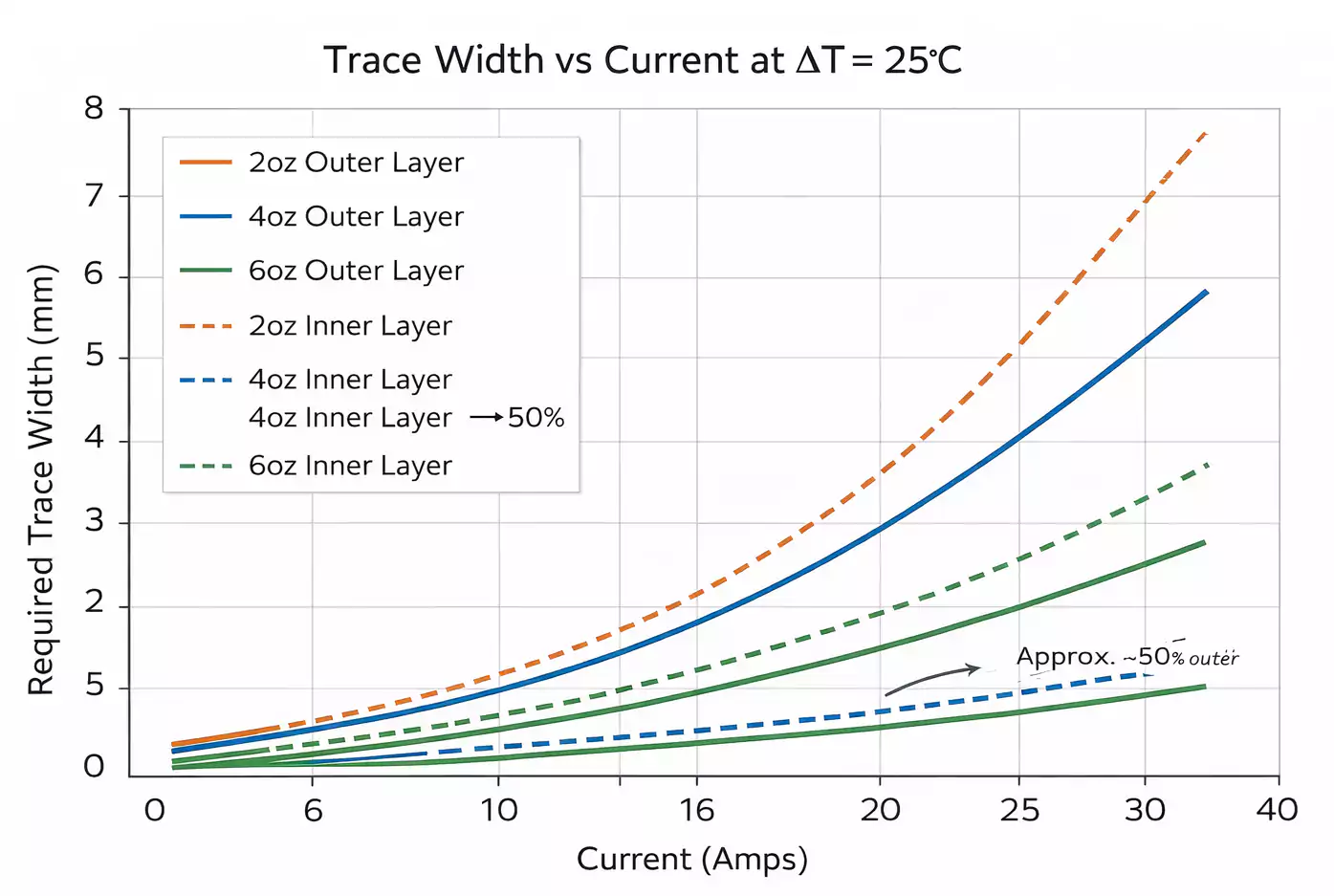
In practical design:
- The outer layers can handle roughly twice the current of the inner layers for the same copper thickness because they cool better.
- Designers often target a temperature rise of 20–30 °C above ambient for continuous operation.
- IPC standards provide formulas and calculators that estimate the required trace width for a given current and copper weight.
Key Manufacturing and Structural Considerations
Controlled Plating and Etching
Thick copper traces are built by controlled heavy-copper plating and precision etching.
Proper process control ensures straight sidewalls and uniform trace geometry even at 10 oz or more.
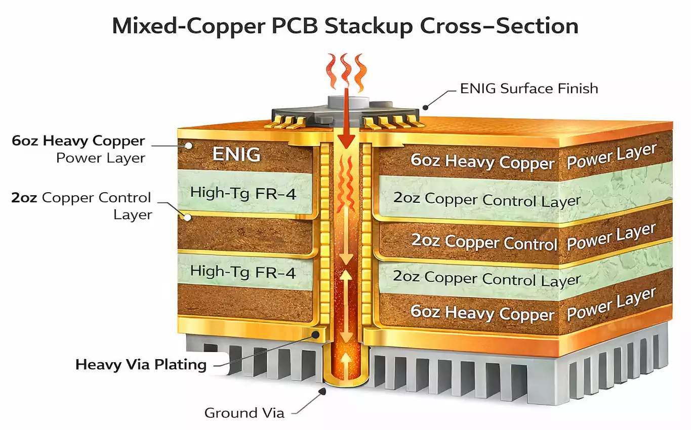
This also allows mixed copper weights on the same board—say, 2 oz for control circuits and 8 oz for power sections.
Drilling and Via Plating
Heavy copper PCBs require thicker via walls to carry current vertically or conduct heat through the board.
Fast Turn PCB uses controlled heavy-copper plating to achieve the desired via copper thickness while maintaining aspect-ratio reliability.
Lamination and Material Selection
For multilayer heavy copper designs, vacuum lamination and high-Tg materials are essential to prevent voids and delamination.
High-Tg FR-4 or specialized high-thermal-conductivity laminates are commonly used to handle repeated heating cycles.
Typical Stackups and Capability Reference
Fast Turn PCB manufactures two- to multilayer thick copper boards with the following capability range:
- Copper thickness: 2 oz – 20 oz+ (both inner and outer layers)
- Board thickness: 0.8 mm – 6 mm typical
- Surface finishes: ENIG, HASL (lead-free), OSP, immersion tin, and others
- Inspection: AOI, X-ray registration, and cross-section analysis for plating and copper thickness verification
- Certifications: ISO 9001, UL, RoHS, and REACH compliant
This broad range enables both prototype and production quantities, with quick-turn options as fast as 2–3 days for time-critical projects.
Common Applications of Heavy Copper PCBs
Heavy copper technology is used wherever high current, reliability, or efficient heat spreading is needed.
Typical industries include:
- Power electronics: converters, inverters, rectifiers, and DC-DC modules
- Automotive and EV systems: chargers, battery management, and motor drives
- Industrial control: power distribution, robotics, and automation drives
- Renewable energy: solar inverters and energy-storage modules
- Aerospace and defense: radar, avionics, power, and rugged mission systems
In these environments, temperature, current, and vibration combine to push standard PCBs to their limits—making thick copper construction a necessity.
Design Tips and Best Practices
Balance Copper Distribution
Large copper areas on one side of the board can cause warpage during lamination and reflow.
Use copper balancing or cross-hatching patterns to maintain even thermal expansion and minimize stress.
Optimize Thermal Paths
Plan for thermal vias under hot components to connect to heavy copper planes or heatsinks.
Avoid trapping heat in inner layers by providing multiple conduction paths to outer copper or metal structures.
Reinforce High-Stress Areas
Connector tabs, screw terminals, and mounting holes benefit from thicker copper and additional plating.
These reinforcements prevent pad lifting and cracking during torque or temperature cycling.
Choose the Right Material
Select high-Tg, low-CTE FR-4 or hybrid laminates that match the copper’s expansion characteristics.
This improves thermal reliability and reduces the risk of delamination or barrel cracking.
Heavy Copper vs. Parallel Copper Layers
When designing for high current, engineers have two main approaches:
- Heavy Copper: Use thick copper on fewer layers.
- Parallel Copper Planes: Use multiple thinner layers carrying current in parallel.
Heavy copper is ideal when space is limited, mechanical strength is critical, or heat must flow quickly to the surface.
Parallel planes may be preferable when fine-pitch routing and signal density are more important.
In many real designs, both methods are combined—outer heavy-copper layers for power and inner standard layers for control and signal routing.
Frequently Asked Questions
1. What qualifies as a Heavy Copper PCB?
Any PCB layer with ≥ 2 oz of copper is heavy copper. Ultra-heavy designs reach 20 oz or more per layer.
2. How much current can a 4-oz copper PCB carry?
It depends on trace width, layer location, and allowable temperature rise. For example, a 4-oz outer trace several millimeters wide can handle tens of amps with a 20–30 °C rise in temperature. Use an IPC trace-width calculator and verify with thermal testing.
3. Can I combine different copper weights on one board?
Yes. Mixed-weight boards—such as 2 oz signal layers with 8 oz power layers—are common. They require specialized plating and etching control, which Fast Turn PCB provides.
4. How is quality controlled?
Every heavy copper PCB undergoes AOI, X-ray alignment, and micro-section analysis. Fast Turn PCB is ISO 9001- and UL-certified, compliant with RoHS.
Final Thoughts
Heavy and thick copper PCBs are the backbone of today’s power electronics.
They handle high current, dissipate heat efficiently, and endure the mechanical and thermal stresses of demanding applications—from EV chargers to aerospace systems.
By choosing an experienced heavy copper PCB manufacturer like Fast Turn PCB, you gain robust manufacturing capability (2–20 oz+ copper, multi-layer builds, ENIG/HASL finishes), prompt engineering feedback, and a 2–3 day prototype turnaround to maintain your schedule.
