


Introduction
As electronic devices shrink and demand more functionality, traditional PCBs can no longer keep up with rising design complexity. Today’s products—smartphones, 5G modules, wearables, automotive systems—require higher I/O counts, tighter spacing, and better signal performance.
HDI PCBs (High-Density Interconnect Printed Circuit Boards) offer a solution. Using advanced features like microvias, blind/buried vias, and laser drilling, HDI boards allow for higher wiring density, smaller form factors, and improved electrical performance.
This guide explains what HDI PCBs are, how they differ from standard PCBs, their key benefits, common layer stack-ups, and core fabrication methods.
What is HDI PCB?
HDI PCB stands for High-Density Interconnect Printed Circuit Board. It uses finer lines, smaller vias, and higher pad density than standard PCBs, enabling more functionality in compact designs.
A key feature is the microvia—a laser-drilled hole typically under 150 μm in diameter—used to connect adjacent layers. HDI designs often include blind and buried vias to increase routing flexibility while maintaining board integrity.
Originally developed to support high I/O density in computing and telecom, HDI technology is now widely used in consumer electronics, automotive systems, medical devices, and aerospace applications where space and performance are critical.
Key Advantages of HDI PCB
HDI PCBs offer several key benefits over traditional multilayer boards:
- Higher Routing Density
HDI boards allow more traces in less space thanks to finer lines, tighter spacing, and microvia technology. This supports high-pin-count components like BGA and CSP packages. - Smaller and Lighter Designs
By reducing layer count and minimizing board size, HDI PCBs help manufacturers create thinner, lighter devices—critical for smartphones, wearables, and medical electronics. - Improved Electrical Performance
Shorter signal paths reduce signal loss, lower inductance, and enhance high-frequency performance. This is essential for RF, high-speed digital, and mixed-signal designs. - Better Thermal and Mechanical Reliability
Staggered or stacked microvias improve mechanical stability and heat dissipation, reducing the risk of failure in harsh or high-power environments. - Enhanced Design Flexibility
Blind and buried vias provide more routing options, enabling compact layouts and complex interconnections without increasing board size.
These advantages make HDI technology a preferred choice for compact, high-performance products in industries like telecommunications, automotive, aerospace, and consumer electronics.
Common HDI Stack‑up Structures
HDI PCB stack-ups define how layers and vias are arranged to achieve high-density routing. Unlike standard multilayer PCBs that rely on through-holes, HDI designs use microvias, blind vias, and buried vias to increase interconnect density without increasing board size.
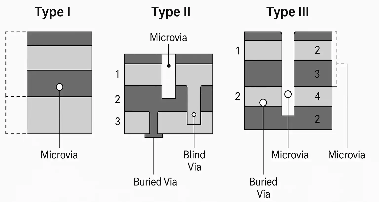
The most common stack-up types are defined by the IPC-2226 standard, which classifies HDI structures into several configurations:
- Type I: One HDI layer on either one or both sides of a core, using blind vias and possibly buried vias, but no via stacking.
- Type II: Similar to Type I but includes plated through-holes (PTHs) from surface to surface.
- Type III: Multiple HDI layers with stacked microvias and buried vias, offering greater density and routing options.
More advanced stack-ups, such as any-layer HDI, allow microvias between all layers. These are used in high-end applications like smartphones, aerospace systems, and miniaturized medical devices.
Choosing the right stack-up depends on design complexity, performance requirements, and cost constraints. For example, Type I may suit consumer electronics, while Type III is better for high-speed, high-reliability systems.
Understanding HDI stack-up structures is essential for optimizing layout, signal integrity, and manufacturability in compact PCB designs.
Core HDI Fabrication Technologies
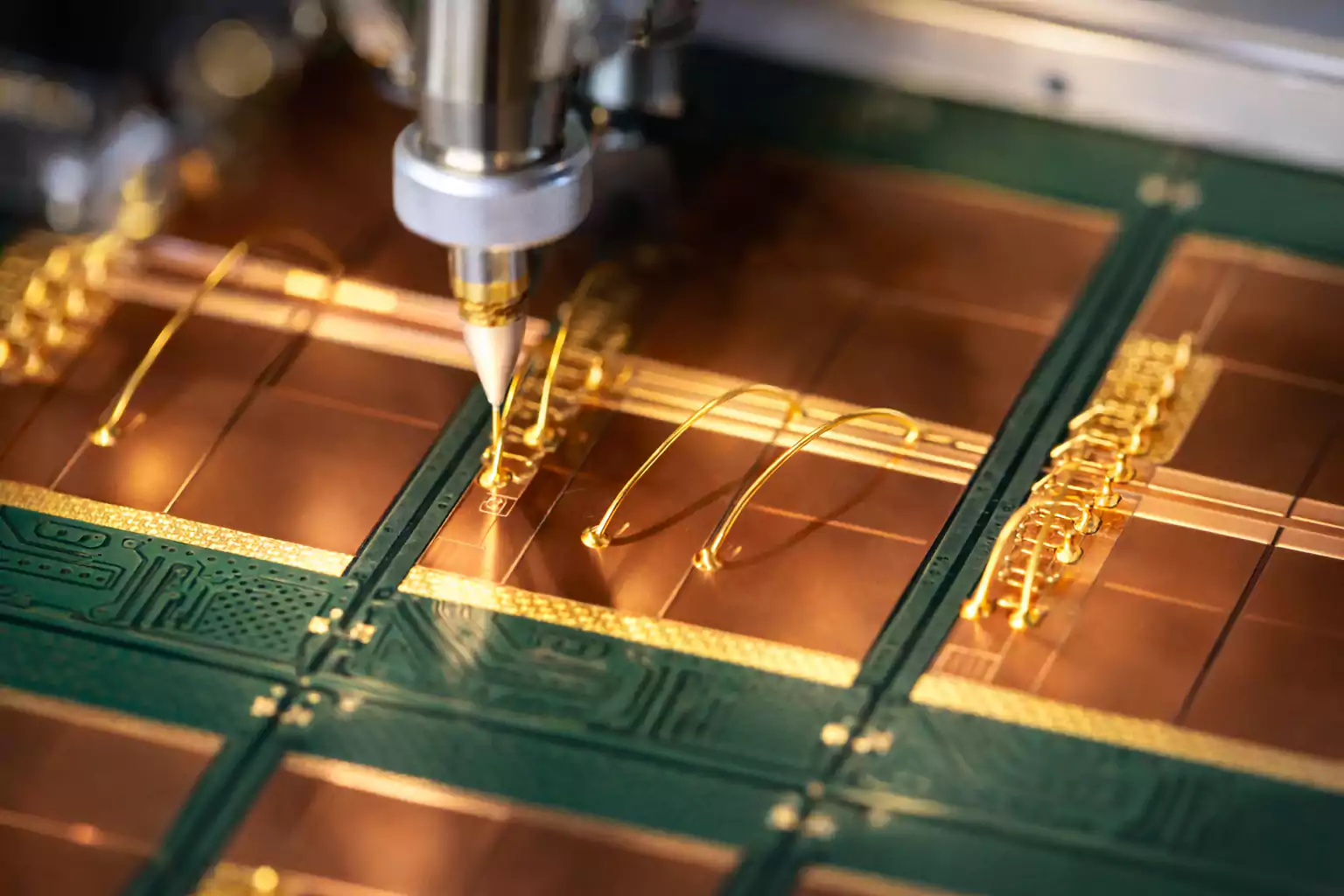
The manufacturing of HDI PCBs relies on specialized processes that enable fine features, precise layer alignment, and reliable interconnections. At the core of HDI fabrication is microvia drilling, which allows for compact, high-density layouts that traditional through-hole processes cannot achieve.
1. Laser Drilling (Primary Method)
Laser drilling is the most common and precise method used to create microvias, typically under 150 μm in diameter. UV or CO₂ lasers selectively ablate the dielectric material to form vias between layers without damaging adjacent areas. This technique supports stacked or staggered via configurations and is ideal for high-volume production.
2. Photo-Defined Microvias
This method uses photoimageable dielectric materials that are exposed and developed similarly to photoresist, then plated to form the vias. It offers good accuracy but is more commonly used in lower-volume or specialized applications.
3. Plasma or Etching Techniques
Plasma etching or chemical methods can also form vias in certain substrates. These are typically used in rigid-flex HDI or for materials sensitive to laser energy.
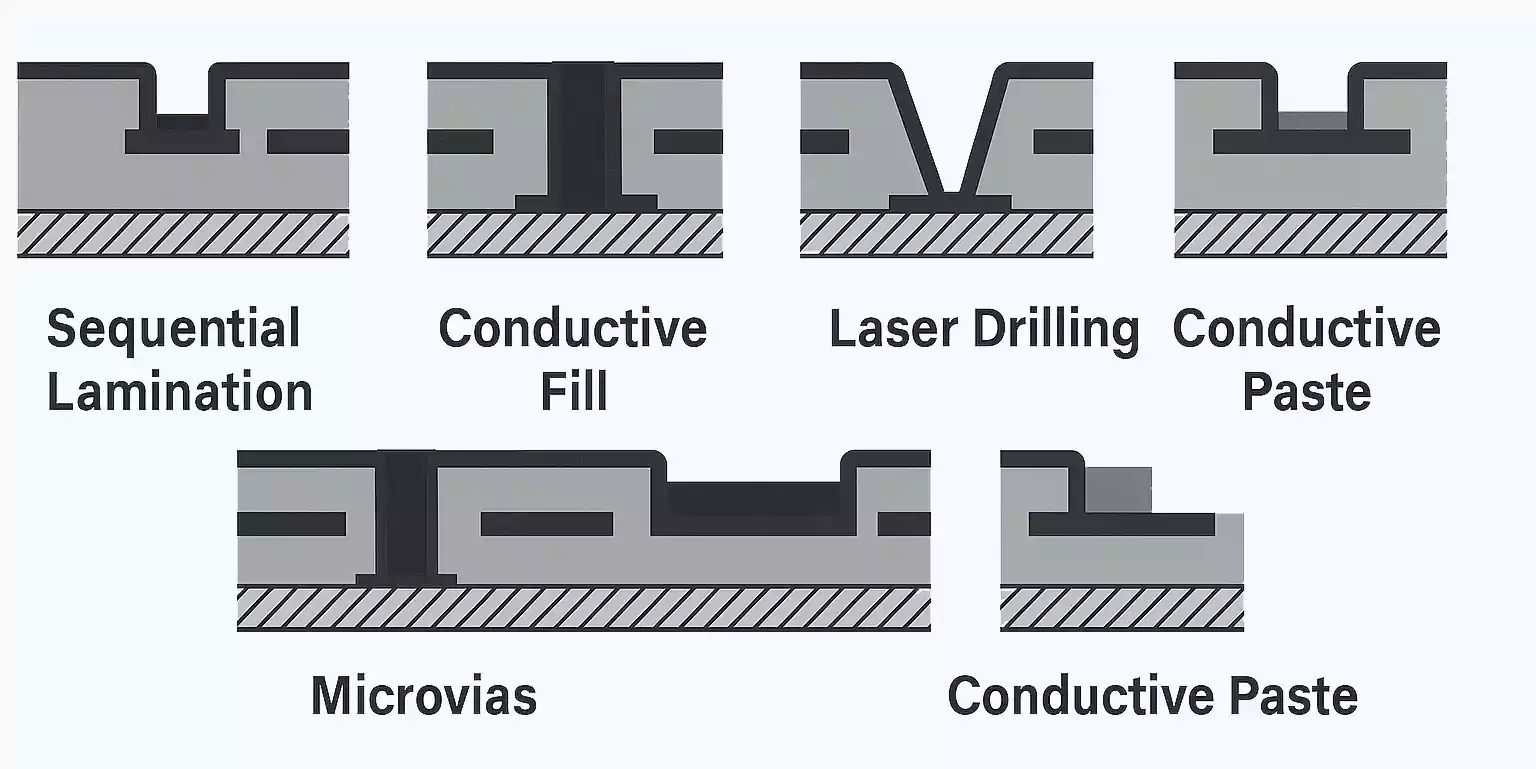
After via formation, the vias are electroplated with copper to establish electrical connections. This step is critical to ensuring conductivity and long-term reliability, especially in stacked or filled microvia structures
At Fast Turn PCB, HDI capabilities include laser-drilled microvias down to 100 μm, line/space as tight as 2.5/2.5 μm, and support for up to 20 layers, enabling advanced high-speed designs up to 28 Gbps.
| Capability | Parameter |
|---|---|
| Min. Line Width/Space | 2.5/2.5 |
| Max. Layer Count | 20 |
| Min. CCL Thickness | 50um |
| Min. Build-Up Thickness | 35um |
| Min. Microvia Design | 100um/200um |
| Min. Finished PTH Size | 0.15mm |
| Impedance Control | Impedance Tolerance: +/-5Ω or +/-10% |
| RoHS Certification | RoHS Certification |
| Lead Free Compliance | Available |
| Green Material - H/F | Available |
| Copper Filled Microvia | Available |
| ELIC Level | 18 Layers |
Industry Standards & Design Guidelines
Designing and manufacturing HDI PCBs requires strict adherence to industry standards to ensure signal integrity, manufacturability, and long-term reliability.
The most widely used HDI standards include:
- IPC-2226 – Sectional Design Standard for HDI Printed Boards
Defines stack-up structures, microvia requirements, and design rules for HDI layers, including via aspect ratios, annular rings, and spacing. - IPC-2315 – Design Guide for High-Density Interconnect Structures
Provides best practices for HDI layout, including routing strategies, microvia placement, and layer optimization to reduce EMI and signal loss. - IPC-4104 – Base Materials for HDI and Microvias
Covers material specifications like resin content, Tg (glass transition temperature), and dielectric performance—critical for high-speed, high-density circuits. - IPC-6016 – Qualification and Performance Specification for HDI PCBs
Establishes performance standards for finished boards, including thermal cycling, reliability, and plating quality.
Following these standards helps ensure your HDI design is compatible with leading PCB manufacturers and meets industry expectations for quality and performance.
Conclusion
HDI PCBs are a practical solution for designs that demand high performance in limited space. With support for fine-pitch components, shorter signal paths, and flexible routing, HDI technology enables reliable, compact circuit boards used across industries such as consumer electronics, automotive, and telecom.
To get the most from HDI, designers should follow IPC standards, apply best practices, and collaborate early with capable manufacturers—especially when using stacked vias or high-layer configurations.