


As PCB designs move toward smaller form factors, higher routing density, and faster performance, conventional through-hole structures are no longer enough for many applications. That is why HDI (High-Density Interconnect) has become a standard approach in modern PCB design.
HDI uses microvias, buildup layers, and fine-line routing to fit more interconnections into less space. In practice, HDI is commonly discussed in terms of PCB types and stack-up structures, from 1+N+1 and 2+N+2 to more advanced formats such as ELIC.
This article explains the main HDI PCB types, how Type I through Type VI structures are defined, what the x[C]x notation means, and how HDI design rules affect manufacturability.
The Core of HDI: Microvias and Routing Density
What defines HDI is its use of microvias and high-density interconnect structures.
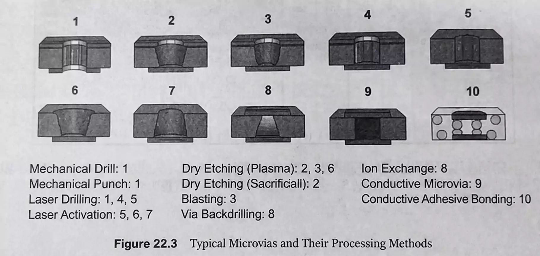
Microvias come in different shapes
Microvias on HDI boards are not limited to a single geometry. Common forms include:
- Straight-wall
- Positive taper
- Negative taper
- Bowl-shaped
These shapes support high-density interlayer connections in compact PCB designs.
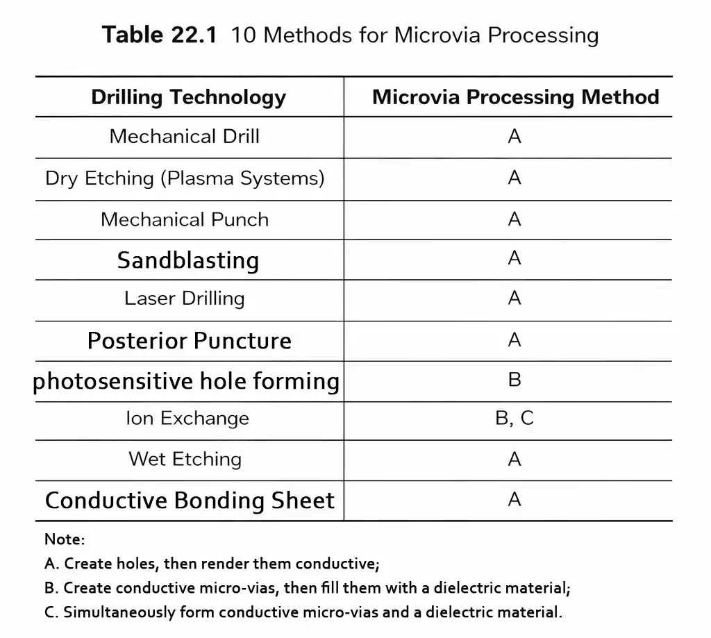
Microvia processing is grouped into three classes
Microvia fabrication is typically classified into:
- Class A
- Class B
- Class C
The processes differ, but the goal is the same: to achieve higher interconnect density in less space.
HDI greatly improves routing density
By combining microvias with buildup layers, HDI can deliver routing density roughly 4 to 8 times higher than conventional through-hole PCB designs.
This is one reason HDI is widely used in:
- Smartphones
- Communication equipment
- Industrial electronics
- High-performance computing systems
IPC classifies microvias into multiple types
In IPC terminology, microvias are not treated as a single generic feature. They are further divided into 10 types, reflecting the range of structures used in HDI design.
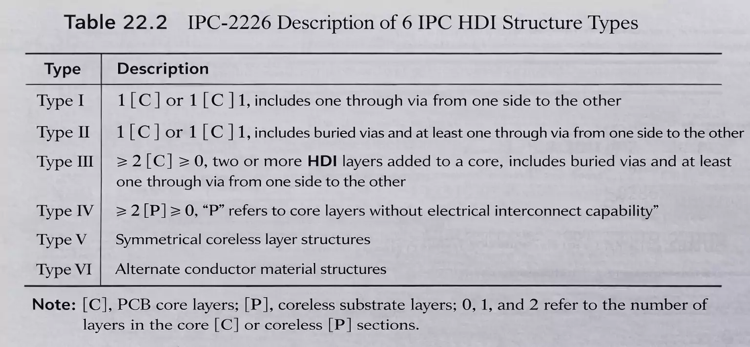
The Basic Classification of HDI PCB Types
HDI structures are generally classified into six main categories:
- Type I
- Type II
- Type III
- Type IV
- Type V
- Type VI
These six categories cover the most common HDI PCB types and HDI stackups currently in use. While new variations may continue to emerge as manufacturing technology advances, this classification system remains the standard framework for understanding HDI structures.
Understanding the Core Layer: What Does [C] Mean?
A key part of HDI structure classification is the core layer.
In HDI notation, [C] represents the core. Depending on its role in the interconnection structure, it can be defined in several ways:
- [CA]: a core with internal conductive vias that can connect to outer layers
- [CB]: a core that supports both internal and external interconnection, with microvias connecting to inner layers
- [CC]: a passive core with no electrical interconnection
This matters because HDI structure is defined not only by buildup layers, but also by the electrical function of the core itself.
What Does x[C]x Mean in HDI Stackup Types?
HDI buildup structures are often described using the notation:
x[C]x
In this format:
- x is the number of buildup layers added to the core
- [C] is an n-layer laminated core, with or without holes
This notation shows how many buildup layers are added to each side of the core.
Examples:
- 1[C]0 = one buildup layer on one side of the core
- 1[C]1 = one buildup layer on both sides
- 2[C]0 = two buildup layers on one side
- 2[C]2 = two buildup layers on both sides
Once this notation is clear, the differences between Type I through Type VI structures become much easier to understand. In practice, it also aligns with common HDI stackup types such as 1+N+1 HDI and other sequential buildup structures.
Main HDI PCB Types
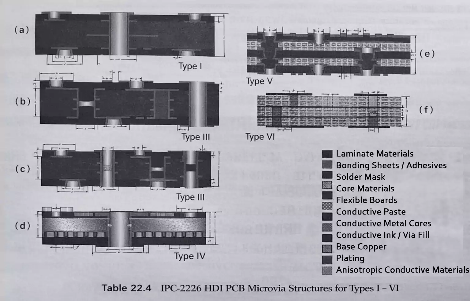
Type I Structure
Common notation
- 1[C]0
- 1[C]1
Key features
Type I includes both metallized microvias and metallized through-holes. Its main feature is a single microvia buildup layer on one or both sides of the core.
- 1[C]0 = one microvia layer on one side
- 1[C]1 = one microvia layer on both sides
Typical structure
Type I starts with a conventional core, which may be rigid or flexible. A dielectric layer is added over the core, and blind vias are formed to connect the outer layers to the adjacent inner layers. Mechanical drilling is then used to create through-holes across the full board thickness. After metallization or conductive filling, the outer-layer circuitry is completed.
How to understand it
Type I is one of the most common and straightforward HDI PCB types. It combines a core, microvias, and plated-through holes in a single-level buildup structure and is closely associated with the 1+N+1 HDI concept.
Type II Structure
Common notation
- 1[C]0
- 1[C]1
Key difference from Type I
Type II has a buildup structure similar to Type I, but the core already contains metallized through-holes before HDI buildup begins.
How to understand it
Type II uses a preprocessed core with plated-through-hole connectivity, then adds an HDI buildup structure on top. It is suitable for designs where part of the interconnection is already built into the core.
Type III Structure
Common notation
- 2[C]0
- 2[C]2
Key features
Type III includes both metallized microvias and metallized through-holes, but adds two microvia buildup layers instead of one.
- 2[C]0 = two buildup layers on one side
- 2[C]2 = two buildup layers on both sides
Typical structure
Type III is typically built by sequential lamination. The first buildup layer forms microvias between adjacent inner layers, followed by metallization and circuit formation. A second dielectric layer is then added to form the outer microvia layer. Through-holes are drilled afterward, and the final circuitry is completed.
Why it matters
Compared with Type I and Type II, Type III supports:
- Higher routing density
- More complex interconnection
- Multi-step buildup structures
It is commonly used in more advanced HDI stackup types.
Type IV Structure
Common notation
- 1[P]0
- 1[P]1
- >2[P]>0
Key features
Type IV is built on a previously drilled and plated substrate rather than an untreated core.
The base structure may be:
- A standard PCB core
- A metal core substrate
- Rigid or flexible
How to understand it
Type IV is best viewed as an HDI structure added to an already processed base with established plated-hole connectivity.
Type V Structure
Key features
Type V is a coreless HDI structure.
Instead of relying on a traditional center core, it connects plated layers or conductive-paste-filled layers through a shared middle layer.
Process characteristic
Layers are typically added in pairs, and interconnections are often formed simultaneously. Unlike standard sequential buildup, Type V is closer to a single lamination process.
How to understand it
Its defining features are:
- No core
- Paired layer construction
- Single-step lamination behavior
This type of coreless HDI is useful where thinner or lighter structures are required.
Type VI Structure
Key features
Type VI is the most flexible HDI category. It allows electrical interconnection and circuit formation to be completed simultaneously, and in some cases, electrical and mechanical structures can also be formed together.
Fabrication options
Type VI may use:
- Sequential lamination
- One-time lamination
Interconnection methods
Unlike conventional HDI, Type VI does not rely only on plating. Interlayer connections may also be formed using:
- Anisotropic films or adhesives
- Conductive paste
- Dielectric piercing methods
- Other non-plated technologies
How to understand it
Type VI represents a more integrated HDI approach, combining interconnection and structure in a single process flow. It is especially relevant in advanced packaging and specialized high-density applications.
HDI Design Rules and Manufacturability
A key difference between HDI design and conventional PCB design is that manufacturing capability directly affects whether the design can be built reliably.
Factory capabilities can vary significantly in areas such as:
- Fine-line imaging
- Etching precision
- Layer-to-layer registration
- Microvia fabrication
- Plating performance
For that reason, HDI design rules are a critical part of real-world HDI development.
Why HDI Design Rules Are Classified
HDI design rules are divided into categories to reflect differences in manufacturing difficulty and producibility.
In general, they can be viewed in two broad manufacturability ranges:
- Preferred manufacturability
- Lower manufacturability
For practical design use, they are commonly simplified into three classes:
- Class A
- Class B
- Class C
This classification approach is closely associated with standards such as IPC-2226, which is widely used in discussions of HDI structures and manufacturability.
What Do Class A, B, and C HDI Design Rules Mean?
Class A: Best for Standard, High-Volume Production
Class A uses relatively relaxed tolerances within standard HDI processes. It offers:
- Lower cost
- Easier yield control
- Better suitability for volume production
- Wider supplier availability
Most HDI-capable manufacturers can support Class A. It is typically the best choice for products that prioritize cost control, stable production, and supply chain flexibility.
Class B: Standard HDI Manufacturing Level
Class B represents a more typical HDI capability level. It requires tighter control than Class A, but remains within the range of most established HDI manufacturers. Roughly 75% of HDI fabricators can support Class B requirements.
Class B is commonly used for:
- Medium- to high-density designs
- Products that need a balance between performance and cost
- Mainstream mid- to high-end electronics
Class C: Advanced Manufacturing Requirement
Class C is the most demanding HDI design category. It requires the highest process capability, and only about 20% of HDI manufacturers can reliably produce it.
To maintain yield, Class C often requires:
- Smaller panel sizes
- Tighter process control
- Special equipment or nonstandard fabrication methods
As a result, it usually comes with:
- Higher cost
- Lower production efficiency
Class C is most often used in advanced applications such as:
- Electronic packaging
- COB (Chip on Board)
- Flip-chip interposers
- MCMs (Multi-Chip Modules)
For most standard PCB production, Class C is not the default choice. It is typically reserved for high-end interconnect and packaging applications.
A Practical Rule in HDI Design
Classes A, B, and C make one thing clear: in HDI design, smaller features are not always better.
A practical design approach should balance:
- Routing density
- Electrical performance
- Manufacturing yield
- Supplier capability
- Production cost
In general, more relaxed design rules are easier to manufacture at scale and cost less. More aggressive rules increase fabrication difficulty, limit supplier options, and raise cost.
Good HDI design is not about pushing every parameter to its minimum. It is about selecting the right structure and design rules for the product and the available manufacturing capability.
HDI Design Rules Must Be Matched to the Structure
HDI design rules should always be evaluated in the context of the structure itself, including:
- The HDI type
- The number of microvia buildup layers
- The design class
- The required manufacturing tolerances
For this reason, design rules are best understood together with a specific HDI structure. A Type III example is often used because its two-level microvia buildup clearly shows the relationship between routing density and manufacturing capability.
Conclusion
HDI is more than a microvia-based PCB concept. It is a complete interconnect system defined by core structure, buildup method, via strategy, and manufacturability.
To understand HDI PCB types, designers need to look at four things together:
- Microvia design
- Structure type
- Stackup notation
- Design rules
In practice, the goal is not to memorize Type I through Type VI. The real value is knowing how to choose the right structure for the application — whether that means a single or multi-stage buildup, a cored or coreless HDI design, or a manufacturable balance between performance and cost.
When structure and manufacturing capability are considered together, HDI design becomes easier to evaluate and more reliable in production.
