

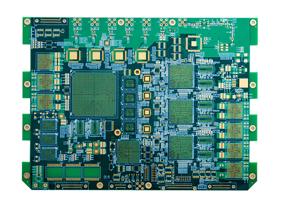
What Is an HDI PCB?
HDI stands for High-Density Interconnect.
An HDI PCB uses fine traces, microvias, and multiple build-up layers to achieve higher wiring density than standard multilayer boards.
According to IPC-2226, an HDI board typically has:
- Trace width and spacing below 100 µm (≈ 4 mil)
- Microvias smaller than 150 µm (≈ 6 mil)
- More than 20 pads per cm² of board area
In simple words, HDI technology allows designers to pack more components in less space, with shorter interconnect paths and better electrical performance — perfect for today’s smartphones, wearables, automotive radar, and medical devices.
HDI Structure Types
HDI structures are defined by the number of microvia layers built over the core.
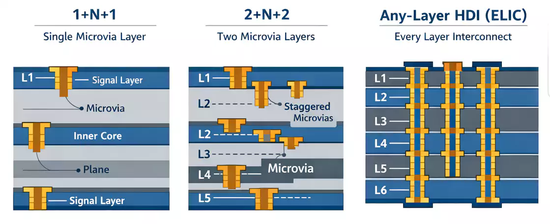
| HDI Type | Description | Typical Use |
| Type I (1+N+1) | One microvia layer on each side of a core | Common in smartphones and IoT boards |
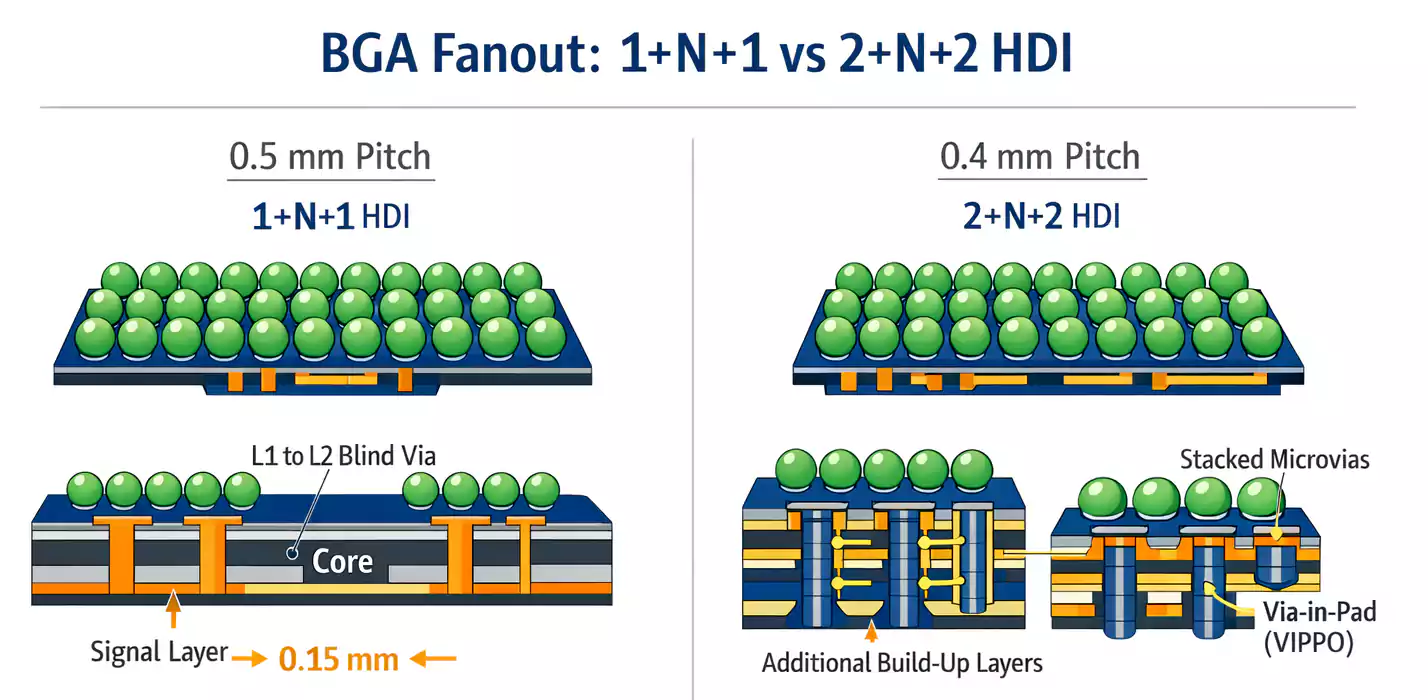
| Type II (2+N+2) | Two microvia layers stacked on each side | Used for dense BGA fan-outs |
| Type III / ELIC (Any-Layer) | Microvias stacked between all layers | Needed for very high-pin-count chips |
Stacked microvias are aligned layer-to-layer, while staggered microvias shift their positions between layers.
Staggered vias are easier and cheaper to manufacture; stacked vias save more space but need stronger plating and inspection.
Typical HDI Stack-ups and Impedance Control
A common 1+N+1 HDI stack-up has one microvia layer on top and one on the bottom, connected to a standard core.
A 2+N+2 adds one more buildup layer on each side.
“Any-layer HDI (ELIC)” connects all layers with stacked microvias for full design flexibility.
Because HDI uses thin dielectrics, impedance control becomes critical.
Signal layers are often paired with solid ground planes close beneath them to maintain controlled impedance for high-speed signals such as PCIe or SerDes.
Microvia and Via-in-Pad Design
Microvias are tiny blind holes created by laser drilling, typically less than 0.1 mm in diameter.
They connect adjacent layers only — for example, layer 1 to 2 or 2 to 3.
Key via types in HDI:
- Blind vias: connect an outer layer to an inner layer.
- Buried vias: connect only the inner layers.
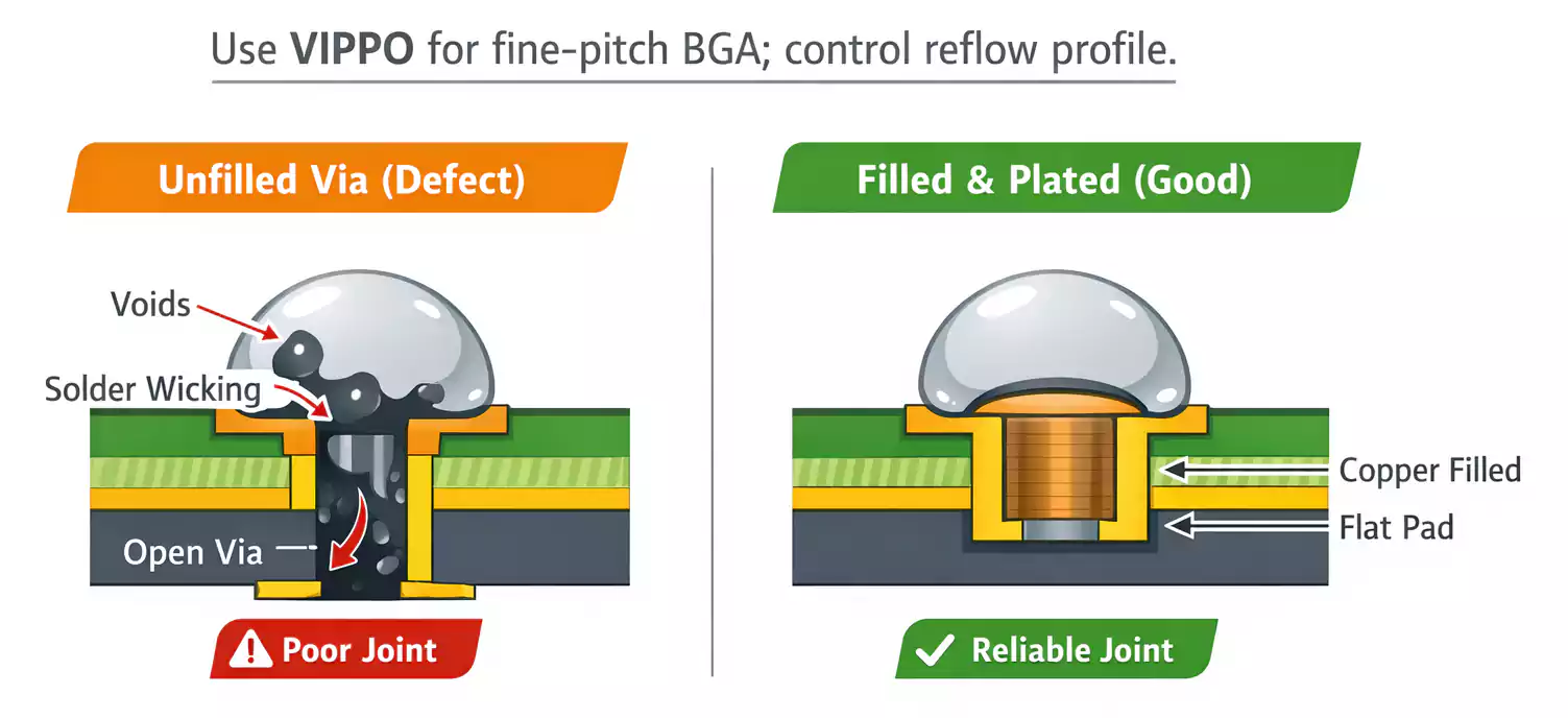
- Via-in-Pad (VIP or VIPPO): placed directly under component pads to save space.
Via-in-Pad designs are popular for fine-pitch BGAs (0.4 mm or below). The vias are filled with copper or epoxy and plated flat, allowing smooth soldering.
However, designers should note:
- Unfilled vias can cause solder wicking during reflow.
- Overstacked microvias increase the risk of plating cracks during thermal cycling.
HDI Manufacturing Process Overview
HDI manufacturing adds layers in steps — a process known as Sequential Build-Up (SBU).
Main steps:
- Core preparation: Drill and plate through-holes for the inner core.
- Build-up layers: Add thin dielectric films (RCC or laser-drillable prepregs).
- Laser drilling: Form microvias (< 0.1 mm).
- Desmear & metallization: Clean and plate via walls.
- Imaging: Use LDI (Laser Direct Imaging) to form ultra-fine traces.
- Copper plating and etching: Build circuit patterns.
- Repeat build-up and lamination for multi-layer HDI.
- Solder mask, surface finish, and testing.
Each extra build-up step increases cost and complexity, so most cost-effective HDI boards use one or two build-ups per side.
Emerging processes such as mSAP (Modified Semi-Additive Process) are pushing line widths below 30 µm for Ultra-HDI designs used in 5G modules and compact RF systems.
Key DFM Rules for HDI Designers
Design-for-Manufacturability (DFM) ensures the design can be built reliably.
Below are general industry-friendly guidelines (actual numbers may vary by supplier):
| Feature | Recommended Value |
| Microvia diameter | 0.075 – 0.10 mm |
| Microvia aspect ratio | ≤ 0.8 : 1 |
| Annular ring (capture pad) | ≥ 0.1 mm |
| Trace / space | 75 – 100 µm |
| Stacked via offset | ≥ 50 µm between vias |
| Finished copper thickness | 18 – 35 µm typical |
| Laser drill tolerance | ± 25 µm |
Avoid over-stacking more than three microvias vertically, as plating reliability drops sharply.
When possible, use staggered or skip vias (layers 1 → 3) to reduce risk and cost.
Signal and Power Integrity in HDI
HDI’s short interconnects reduce parasitic capacitance and inductance, which improves signal integrity.
Benefits:
- Fewer stubs → less reflection
- Shorter return paths → lower loop area
- Denser power-ground pairs → lower noise
Design tips:
- Keep reference planes solid under high-speed traces.
- Use stitching vias near plane splits or edges.
- For differential pairs, keep consistent spacing even across microvias.
- Simulate impedance early, as dielectric thickness tolerance is smaller in HDI builds.
Reliability and Testing
Because HDI boards use thin dielectrics and fine vias, reliability testing is essential.
Common issues:
- Neck cracking in stacked microvias due to repeated thermal stress.
- Copper fatigue from multiple reflow cycles.
- CAF (Conductive Anodic Filament) growth occurs if resin and glass are not properly matched.
Validation methods:
- IST (Interconnect Stress Test)
- Thermal shock / cycle testing
- X-ray and cross-section inspection
High-reliability markets (automotive, aerospace, defence) require extra qualification for via fill and plating quality.
Material Selection for HDI
Choosing the right material affects both manufacturability and signal performance.
Common materials:
- RCC (Resin-Coated Copper) enables thin, laser-drillable dielectrics.
- Laser-drillable prepregs: improve adhesion between buildup layers.
- Spread-glass laminates: provide better dimensional stability.
- Low-loss materials (Df < 0.005): necessary for high-speed SerDes (> 10 GHz).
Look for a balanced CTE (Coefficient of Thermal Expansion) and a high Tg (> 170 °C) to withstand multiple lamination and soldering cycles.
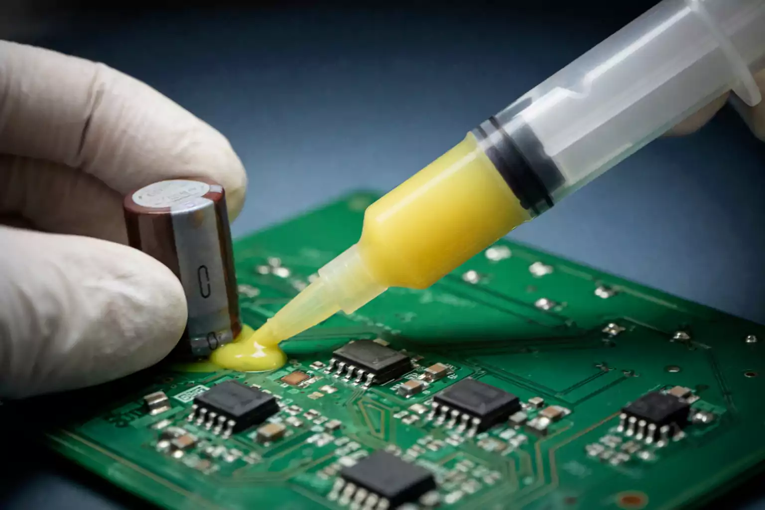
HDI and SMT Assembly Considerations
During Surface-Mount (SMT) assembly, HDI introduces special challenges.
- Via-in-Pad: must be filled and plated flat to prevent solder voids or wicking.
- Solder mask plugging: seals vias under BGAs to avoid air bubbles.
- Stencil design: Use step stencils or smaller apertures for tiny parts (0201 / 01005).
- Reflow profile: control heating rate to protect thin HDI cores from warping.
Because components are closer and copper distribution is tighter, thermal management during reflow is also important.
Typical Design Mistakes and Fixes
| Design Issue | Manufacturing Effect | Recommended Fix |
| Too many stacked microvias | Cracking during plating | Use staggered vias or fewer buildup layers |
| Via-in-Pad not filled | Solder wicking, poor joints | Use copper-filled or epoxy-filled VIPPO |
| Insufficient annular ring | Drill breakout | Increase capture pad size |
| Thin core without support | Warp during lamination | Add balancing layers or thicker prepreg |
| Small isolation around microvias | Etching shorts | Increase clearance or adjust design rules |
Key Terms
| Term | Meaning |
| HDI | High-Density Interconnect |
| Microvia | Laser-drilled via connecting only two layers |
| Blind Via | Via from outer layer to an inner layer |
| Buried Via | Via between inner layers only |
| Via-in-Pad (VIP / VIPPO) | Via placed in component pad, filled and plated over |
| SBU | Sequential Build-Up process |
| ELIC | Every Layer Interconnect (Any-Layer HDI) |
| mSAP | Modified Semi-Additive Process for ultra-fine lines |
Conclusion
HDI PCB technology enables compact and reliable electronic designs.
Through fine-line etching, optimized stack-ups, and controlled via structures, it supports high-speed performance in limited space.
At Fastturn PCB, we build HDI boards with mechanical micro-drilling, LDI imaging, and multi-layer lamination for communication, automotive, and consumer applications.
Capabilities:
- Via size: 0.10 mm (mechanical)
- Trace/space: 0.075 mm
- Up to 20 layers
- Via filling and plating
