Introduction
PCB plating is essential for ensuring reliable electrical connections and durable surfaces in circuit board manufacturing. It serves two key functions: forming conductive paths in through-holes and applying surface finishes that protect exposed copper and support solderability.
In this guide, you'll learn how through-hole copper plating works, the differences between electroless and electrolytic processes, and how to choose the right surface finish—such as HASL, ENIG, OSP, or immersion silver—based on your application.
Whether you're designing, sourcing, or assembling PCBs, understanding these plating processes helps ensure performance, longevity, and cost-efficiency.
PCB Through‑Hole Copper Plating Process Overview
Through-hole copper plating is a critical step in multilayer PCB manufacturing that ensures reliable electrical connections between layers. The process involves depositing a conductive copper layer inside the drilled holes (vias) of the PCB, enabling current to flow from one layer to another. This section outlines the full process—from pre-treatment to final copper deposition—along with key technical considerations for optimal performance.
1. Cleaning and Desmearing
Before any copper can be deposited, the freshly drilled holes must be thoroughly cleaned. Mechanical drilling often leaves behind debris, resin smears, and oxidation, all of which can interfere with plating adhesion.
- Desmearing: Performed using plasma or chemical treatment (e.g., permanganate solution), this step removes resin residue from the hole walls.
- Surface Preparation: The inner copper layers and hole walls are micro-etched to improve bonding and wettability for the plating process.
This stage is essential for ensuring the electroless copper adheres uniformly and avoids plating voids or delamination.
2. Electroless Copper Plating (Chemical Plating)
Also known as PTH (Plated Through Hole) activation, this step deposits a thin, conductive copper layer inside non-conductive drilled holes without using electricity.
- Catalyst Activation: The board is immersed in a palladium-based solution to activate the insulating surfaces.
- Chemical Deposition: Copper ions are reduced from the solution and deposited evenly on all hole walls and exposed copper areas.
Typical electroless copper thickness ranges from 0.5 to 1.0 µm, forming a conductive base layer for subsequent electroplating. This layer is critical for establishing reliable vias and preventing open circuits in multilayer boards.
3. Electrolytic Copper Plating (Electroplating)
Once the conductive layer is established, electrolytic plating builds up the copper thickness both inside the holes and on the PCB surface.
- Electroplating Setup: The PCB is connected to a cathode bus bar and submerged in an acidic copper sulfate solution.
- Additives in Bath: The solution contains brighteners, levelers, and suppressors to ensure uniform deposition and high-quality surface finish.
- Current Application: A controlled DC current facilitates copper ion deposition from the anode onto the PCB.
The electroplated copper thickness is usually 18–25 µm (0.7–1.0 mil) for standard applications, meeting IPC-6012 Class 2/3 requirements. For high-reliability designs, additional thickness may be applied.
4. Wrap Plating (Edge Coverage)
To enhance electrical reliability—especially in via-in-pad or HDI structures—wrap plating is employed to extend the plated copper around the hole walls and slightly onto the surface.
- IPC-6012B mandates that plated copper wraps at least 0.025 mm (1 mil) from the hole onto the surrounding land area.
- Proper wrap plating improves solder joint strength and reduces the risk of pad lifting during assembly or rework.
5. Quality Control and Thickness Testing
Consistent copper thickness and coverage are essential for performance and longevity. Common inspection and test methods include:
- Microsection Analysis: Cross-sectional inspection under a microscope to verify plating uniformity and thickness.
- X-Ray Fluorescence (XRF): Non-destructive testing to measure copper deposition across the board.
- Adhesion Testing: Ensures plating layers are bonded well to the substrate and will withstand thermal and mechanical stress.
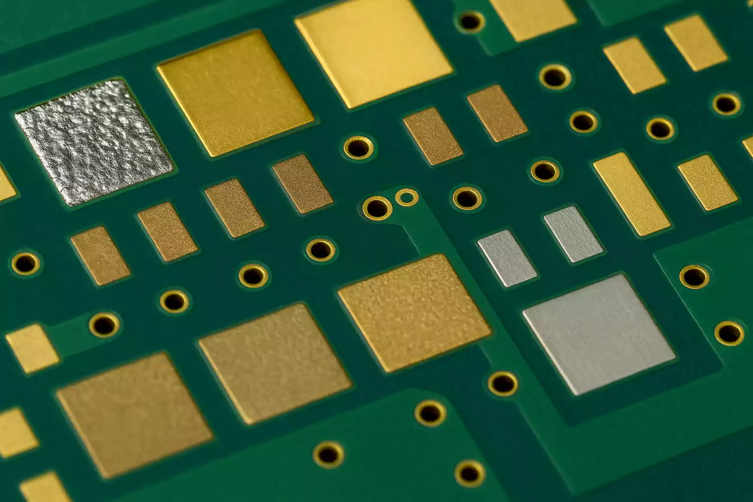
Comprehensive Guide to PCB Surface Finishes
PCB surface finishes serve as a protective coating over exposed copper pads and traces, preserving solderability and preventing oxidation. Choosing the right surface finish directly affects manufacturing yield, long-term reliability, and cost. This section outlines the most common surface finishes, comparing their properties, use cases, pros and cons, and how to choose the ideal one for your application.
1. HASL (Hot Air Solder Leveling)
Overview: HASL is one of the oldest and most cost-effective finishes, where the PCB is dipped into molten solder and then leveled using hot air knives.
Key Features:
- Available in lead-free and lead-based versions
- Good shelf life and solderability
- Suitable for through-hole and large component assemblies
Limitations:
- Uneven surface; not ideal for fine-pitch SMD components
- Thermal shock during processing
- Not recommended for high-frequency or impedance-controlled designs
Best For: General-purpose boards, through-hole PCBs, cost-sensitive applications
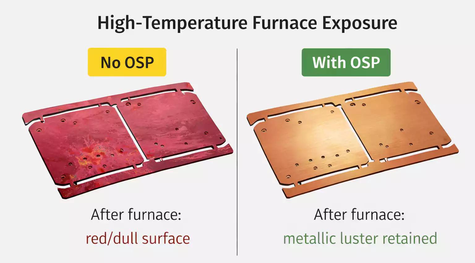
2. OSP (Organic Solderability Preservative)
Overview: OSP applies a thin, organic compound (usually azole-based) to protect the copper from oxidation while preserving excellent solderability.
Key Features:
- Flat, smooth surface—ideal for fine-pitch SMDs and BGA components
- Lead-free and RoHS-compliant
- Excellent for single reflow cycles
Limitations:
- Shorter shelf life (usually 6–12 months)
- Poor durability for multiple reflows or high-temperature processing
- Easily scratched, requiring careful handling
Best For: High-volume, single-reflow SMT production; consumer electronics
3. Immersion Tin (ISn)
Overview: A metallic tin layer is chemically deposited on copper, forming a flat and solderable surface without lead.
Key Features:
- Flat surface finish with good solderability
- Suitable for press-fit components
- Compatible with RoHS requirements
Limitations:
- Tin whiskers may form, leading to potential shorts
- Not recommended for multiple assembly cycles
- Sensitive to handling and storage conditions
Best For: Telecom, backplane, and connector-heavy designs
4. Immersion Silver (IAg)
Overview: Immersion silver offers a thin silver layer over copper with excellent conductivity and surface planarity.
Key Features:
- High-frequency signal performance
- Excellent wettability and flatness
- Cost-effective compared to gold-based finishes
Limitations:
- Tarnishes easily if not stored properly
- May require nitrogen environment during reflow
- Silver migration under high humidity
Best For: RF boards, high-speed digital circuits, and fine-pitch SMT assemblies
5. ENIG (Electroless Nickel Immersion Gold)
Overview: ENIG applies a two-layer finish with a nickel barrier (for preventing copper diffusion) and a thin gold topcoat (for solderability).
Key Features:
- Excellent surface flatness—ideal for BGA, QFN, and HDI designs
- Long shelf life (12+ months)
- Suitable for multiple reflow cycles
Limitations:
- More expensive than OSP or HASL
- Risk of “Black Pad” defect if plating isn’t tightly controlled
- Slightly brittle solder joints compared to tin finishes
Best For: High-reliability, high-density applications in aerospace, medical, and telecommunications
6. ENEPIG (Electroless Nickel Electroless Palladium Immersion Gold)
Overview: ENEPIG adds a palladium layer between nickel and gold, improving oxidation resistance and preventing “Black Pad.”
Key Features:
- Superior wire bonding compatibility (gold and aluminum)
- Excellent corrosion resistance
- Long shelf life and solderability
Limitations:
- Higher cost due to multiple precious metal layers
- Requires precise process control
Best For: Mission-critical electronics, wire bonding, military and aerospace PCBs
7.Surface Finish Selection Guide
| Finish | Flatness | Cost | Shelf Life | Solderability | Best For |
|---|---|---|---|---|---|
| HASL | Low | Low | High | Good | General-purpose, through-hole |
| OSP | High | Low | Moderate | Excellent (1x) | High-volume SMT |
| Imm. Tin | High | Medium | Moderate | Good | Connectors, press-fit |
| Imm. Silver | High | Medium | Low–Mod. | Excellent | RF / high-speed boards |
| ENIG | Very High | High | High | Excellent | HDI, fine-pitch, BGA |
| ENEPIG | Very High | Very High | High | Excellent | Aerospace, wire bonding |
Process Parameters and Standards Quick Reference
Accurate control of plating parameters and strict adherence to industry standards are vital for ensuring consistent quality, electrical performance, and long-term reliability in PCB fabrication. This section provides a quick-reference guide to the key copper plating and surface finish parameters, as well as essential IPC standards that govern PCB plating processes.
1. Typical Copper Plating Thickness Guidelines
| Application Area | Process | Typical Copper Thickness | Relevant Standards |
|---|---|---|---|
| Through-Hole Vias (PTH) | Electrolytic Copper Plating | 18–25 µm (0.7–1.0 mil) | IPC-6012, IPC-2221 |
| Internal Layer Traces | Copper Foil Lamination | 18–35 µm (0.7–1.4 mil) | IPC-2221, IPC-6011 |
| Outer Layer Traces | Electrolytic Copper + Plating | 35–70 µm (1.4–2.8 mil) | IPC-6012 Class 2/3 |
| Wrap Plating Around Vias | Edge Wrap Requirement | ≥ 25 µm (1.0 mil) | IPC-6012B (Wrap Plating Spec) |
| Surface Finishes (e.g., ENIG) | Nickel Layer | 3–6 µm (120–240 µin) | IPC-4552, JEDEC J-STD-003C |
| Gold Layer (Electroless) | 0.05–0.1 µm (2–4 µin) | IPC-4552 | |
| ENEPIG Finish | Palladium Layer | 0.05–0.1 µm (2–4 µin) | IPC-4556 |
2.Key IPC Standards for PCB Plating and Finishing
Understanding and applying the correct IPC standards is essential for product quality, especially in high-reliability or regulated industries. Below are the most relevant specifications for copper plating and surface finishes:
| Standard | Title | Scope |
|---|---|---|
| IPC-6012 | Qualification and Performance for Rigid PCBs | Defines plating thickness, via integrity, and wrap requirements |
| IPC-2221 | Generic PCB Design Standard | Specifies design requirements for copper weights and trace widths |
| IPC-6011 | Generic Performance Specification for PCBs | Basic quality metrics for copper conductors and structural integrity |
| IPC-4552 | Specification for ENIG Surface Finish | Covers Ni/Au thickness and quality for electroless nickel immersion gold |
| IPC-4556 | Specification for ENEPIG Finish | Requirements for electroless nickel, electroless palladium, immersion gold |
| IPC-A-600 | Acceptability of Printed Boards | Visual criteria for plating voids, thickness uniformity, and finish defects |
| IPC-TM-650 | Test Methods Manual | Includes microsectioning and copper thickness measurement procedures |
3.Essential Plating Process Control Parameters
For manufacturers aiming to deliver consistent, high-reliability boards, real-time process control is crucial. Key parameters include:
- Current Density: Typically 1.5–3.0 A/dm² for electrolytic copper plating
- Bath Temperature: 20–25 °C (68–77 °F) for acid copper solutions
- Agitation: Mechanical or air sparging to maintain solution uniformity
- pH Level: Maintained around 0.2–1.0 for optimal copper ion availability
- Additive Control: Levelers and brighteners must be carefully dosed to prevent roughness or uneven plating
- Plating Time: Adjusted based on desired copper build-up and board thickness
4. Plating Thickness Tolerance and Uniformity Expectations
- Copper Thickness Tolerance: ±20% is typical for internal and external layers
- Hole Wall Uniformity: Must meet minimum IPC-6012 requirements (≥20 µm in critical vias)
- Surface Finish Consistency: Gold or silver layer uniformity critical for solderability and contact resistance
Frequently Asked Questions (FAQ)
What is the difference between electroless and electrolytic copper plating?
Electroless plating uses a chemical process to deposit copper without electricity—ideal for activating non-conductive hole walls.
Electrolytic plating uses electric current to build up copper thickness after electroless activation.
How thick should copper be inside a plated through-hole (PTH)?
Per IPC-6012 standards, the minimum copper thickness inside a PTH is typically 20–25 µm (0.8–1.0 mil) for Class 2 boards. Higher reliability boards may require more.
Which surface finish is best for high-frequency PCBs?
ENIG or Immersion Silver are preferred for RF and high-speed PCBs due to their flatness and low signal loss. HASL is not recommended for these applications.
What is black pad in ENIG, and how can it be prevented?
Black pad is a corrosion defect in the nickel layer during ENIG processing, causing poor solderability. Prevention includes tight control of pH, immersion time, and using high-purity chemistry.
How does OSP compare to ENIG?
OSP is cost-effective and good for short-term builds.
ENIG offers better shelf life, oxidation resistance, and compatibility with fine-pitch components, making it ideal for complex or long-life products.
What is wrap plating, and why is it important?
Wrap plating extends copper from the hole barrel onto the pad surface, improving solder joint strength and electrical contact.
IPC-6012B recommends at least 0.025 mm (1 mil) of wrap coverage.
Is thicker copper plating always better?
No. While thicker copper increases current capacity and durability, it may reduce etching precision and raise costs. Choose thickness based on your design's electrical and thermal needs.
Conclusion: Mastering PCB Plating for Reliability and Performance
Through-hole copper plating and surface finish selection are two of the most critical processes in printed circuit board (PCB) manufacturing. When executed correctly, they ensure long-term electrical connectivity, structural integrity, and solderability—all of which are essential for high-performance electronics.
Understanding the full plating process—from cleaning and electroless copper activation to electrolytic plating and final surface treatment—empowers engineers and procurement teams to make informed decisions. Equally important is selecting the right surface finish, whether it's ENIG for fine-pitch components, HASL for cost-effective applications, or OSP for lead-free compliance.