


When you look at a modern graphics card, the first thing you notice is often the big heatsink or colorful lighting. But underneath it all, the real star is the graphics card PCB—the printed circuit board that holds, powers, and connects every critical component. Today, we’ll break down what makes a graphics card PCB unique, why it’s so complex, and how engineering choices around layers, impedance, BGA assembly, and thermal design impact performance.
What Is a Graphics Card PCB?
A graphics card PCB connects the GPU, memory chips, power circuits, and all other parts. Far beyond a piece of fiberglass with copper tracks, it’s a dense, multi-layer platform for fast data transfer and precise power delivery—think of the PCB as an integrated road network, power grid, and foundation.
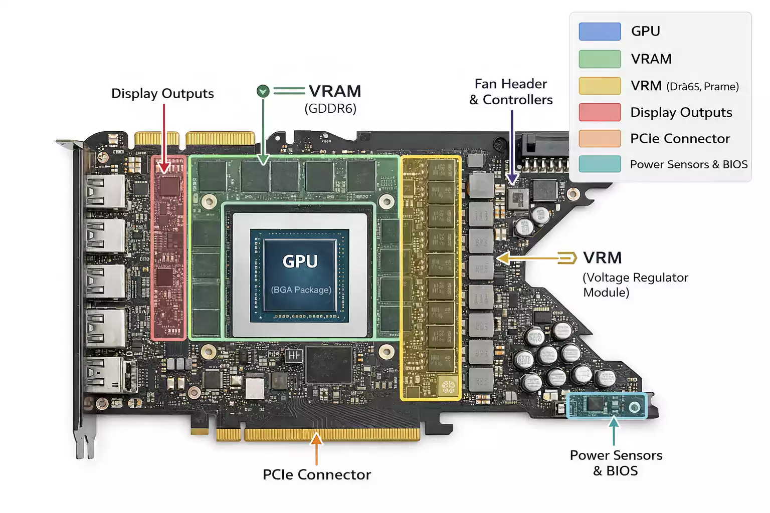
Main functional areas on a graphics card PCB include:
- GPU BGA Zone: The main processor chip, mounted with a grid of solder balls (BGA).
- Memory Area: Usually, GDDR chips are placed around the GPU.
- VRM (Voltage Regulator Module) Area: Power delivery components like MOSFETs, chokes, and capacitors.
- PCIe Edge (Golden Fingers): Connects to your motherboard.
- Display Output Area: HDMI, DisplayPort, or DVI connectors.
- Sensors & Monitoring: Circuits to check voltage, temperature, and fan control.
PCB Difference from a Full Graphics Card:
The PCB is the board with electronics; the full card also includes the heatsink, fans, shroud, and possibly a backplate. The PCB is the foundation that supports everything.
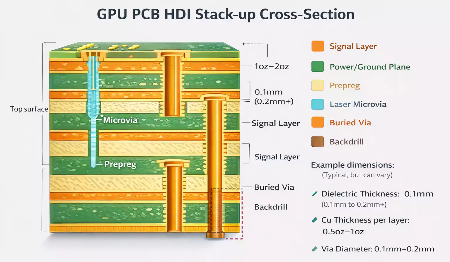
Why So Many Layers? HDI Stack-Up in GPU PCBs
Unlike simple PCBs in remote controls or toys, graphics card PCBs are “multi-layer” or even “HDI” (High-Density Interconnect) boards. High-end GPUs may have 8, 10, or even 14+ copper layers inside the board, each separated by insulating material.
Why so many layers?
- Signal Routing: PCIe, GDDR, and other high-speed signals require dedicated tracks and ground planes to control interference.
- Power Delivery: Wide copper pours and separate power/ground layers for GPU and memory ensure stable voltage.
- High Density: More components and connections need more “real estate”—extra layers let engineers pack more into the same area.
- EMI Control: Extra layers help shield against electromagnetic interference, which is critical at modern speeds.
HDI Techniques:
- Microvias: Tiny laser-drilled holes connecting only two or three adjacent layers (unlike traditional “through-holes” that pass all the way through).
- Blind/Buried Vias: Vias that connect only partway through the board, saving space.
- Backdrilling: Removing unused via stubs to improve signal integrity at very high speeds.
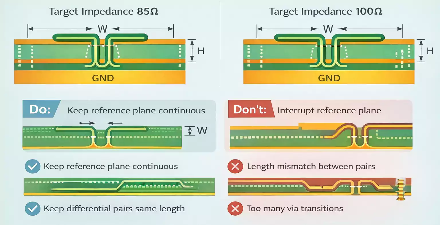
Impedance Control and High-Speed Routing
When signals move at gigahertz speeds, as in PCIe Gen4/5 or GDDR6 memory, even tiny electrical mismatches can cause errors. That’s why controlled impedance and smart routing are so important.
What is Impedance?
Impedance, measured in ohms (Ω), describes how a PCB track resists the flow of fast electrical signals. Each pair of differential traces (like PCIe or GDDR data lines) must be designed for a target impedance—usually 85Ω or 100Ω. If the actual impedance strays too far from this, signals get reflected, blurred, or lost.
How Engineers Control Impedance:
- Trace Width/Spacing: Wider traces or closer pair spacing change impedance.
- Dielectric Thickness: The distance from the trace to the ground layer is important.
- Material Consistency: Using stable, high-Tg FR-4 or better materials helps keep impedance predictable.
- Layer Stack-Up: Having a continuous ground plane under each signal layer.
High-Speed Routing Rules:
- Keep differential pairs (like PCIe) close and parallel for matching.
- Match the length of all traces in a bus (to avoid timing errors).
- Minimize the number of vias (holes), bends, and splits in ground planes.
BGA Assembly: The GPU and GDDR Challenge
The GPU and video memory (GDDR) chips use BGA (Ball Grid Array) packages—hundreds or thousands of tiny solder balls connecting the chip to the PCB.
Why BGA?
- Allows dense connections in a small area.
- Shorter connections mean less electrical noise and better performance.
Assembly Challenges:
- Pad Design: There are two main types—NSMD (Non-Solder Mask Defined) and SMD (Solder Mask Defined). NSMD pads are common for BGA because they give more reliable solder joints.
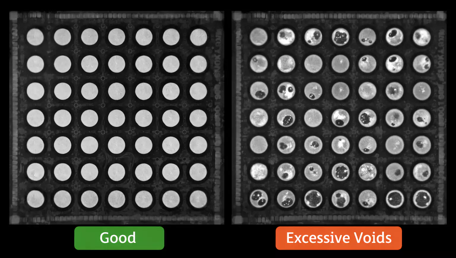
- Soldering & Reflow: The whole board is heated in a reflow oven. If the PCB isn’t flat or the solder profile is off, solder balls may fail to make contact or form voids (air pockets).
- Void Control: Too many voids (typically over 25% area) weaken joints. Advanced factories target under 10% (or even 5% for premium GPUs), verified by X-ray inspection.
- Warpage: Thick or uneven PCBs can bend during assembly, causing “cold joints” or open circuits.
Power Delivery & VRM Thermal Design
Modern GPUs can draw hundreds of watts. The VRM (Voltage Regulator Module) section of the PCB must supply high currents while minimizing losses and keeping the module cool.
Key VRM PCB Design Points:
- Component Layout: MOSFETs, inductors, and capacitors are arranged for the shortest, lowest-resistance loops.
- Copper Thickness: Thicker copper (sometimes 2oz or more) helps carry current and spread heat.
- Thermal Vias: Rows of small holes filled with copper connect the top and bottom layers, pulling heat away from hotspots.
- Backplate Contact: High-power cards often use a thermal pad between the PCB and a metal backplate to improve heat dissipation.
If the VRM overheats, it throttles performance or causes crashes. Good PCB design is the first line of defense—before the heatsink even comes into play.
Structural Reliability & Testing
A graphics card PCB must survive the stress of heatsink mounting, temperature swings, and the pull of PCIe slots. Structural reliability comes from material choices, board thickness, and smart placement of mounting holes.
Testing Steps Before Shipping:
- AOI (Automated Optical Inspection): Cameras check for missing parts or solder issues.
- Electrical Test (Flying Probe/Bed of Nails): Checks that every connection works.
- X-Ray Inspection: Especially for hidden BGA joints.
- Functional Test: Ensures the GPU powers up and works with real data.
Common FAQs
1. How many layers does a typical graphics card PCB have?
High-end GPUs often use 8–14 layers, sometimes more. More layers mean better routing, power delivery, and signal control, all of which are needed for today’s fast, complex chips.
2. What’s the difference between the GPU PCB and a full graphics card?
The PCB is just the board and components. The full card adds the cooler, shroud, backplate, and display outputs.
3. Why is impedance control so important?
Because high-speed signals (PCIe, GDDR) are very sensitive to electrical mismatches. Bad impedance = unreliable data or crashes.
4. What are typical BGA void limits?
Most factories set a maximum allowed void area of 25% per solder ball. Top-tier GPU lines target under 10% (even 5%) for long-term reliability.
Conclusion
Graphics card PCBs are true engineering marvels. They need to handle high power, ultra-fast data, and mechanical stress—all in a tight, reliable package. Layer stack-up, impedance, BGA soldering, and thermal management are the pillars of their performance. Next time you admire a powerful GPU, remember: it’s the PCB under the hood that holds everything together.
If you want to learn more about PCB engineering, or need HDI prototypes or assembly for your own designs, check out FastTurnPCB for expert help.
