How Is a PCB Manufactured?
Printed Circuit Board (PCB) manufacturing transforms electronic design files—such as Gerber, ODB++, or IPC-2581 formats—into physical circuit boards that form the backbone of nearly every electronic product.
The process begins once the layout and schematic files are finalized. These digital blueprints are reviewed for manufacturability and translated into tooling data for fabrication. Through a series of precisely controlled steps—including inner layer imaging, etching, lamination, drilling, plating, solder mask application, and surface finishing—the PCB takes shape layer by layer.
After fabrication, the bare board proceeds to component assembly and electrical testing, completing the transition from digital concept to functional hardware.
This guide provides a comprehensive, step-by-step overview of the PCB manufacturing process. Whether you're a design engineer, project manager, or electronics enthusiast, understanding these steps will help you communicate better with your manufacturer, optimize your designs for production, and ensure higher reliability in your end product.

Pre-production Engineering
The PCB manufacturing process begins once the design files are received from the PCB designer or electronics engineer. These files include:
- Gerber, ODB++, or IPC-2581 formats, which contain all the graphical and layer data required for fabrication.
- Drill files specifying hole locations, sizes, and types (via, through-hole, etc.).
- Netlists used for electrical testing and verification.
- Bill of Materials (BOM) and Pick-and-Place files (for downstream assembly, if applicable).
At this stage, manufacturers validate the design for manufacturability and prepare all necessary files for production. This step is critical to ensuring accuracy, yield, and cost-efficiency.
Key Processes in Pre-production Engineering:
Design for Manufacturability (DFM) Checks
Engineers inspect the files to detect potential issues that could impact fabrication or yield. Common checks include:
- Minimum trace width and spacing violations
- Copper-to-edge clearances
- Drill-to-copper distances
- Solder mask slivers or insufficient mask openings
Any errors or concerns are reported back to the customer for revision or approval, preventing costly downstream delays.
Computer-Aided Manufacturing (CAM) Processing
After DFM clearance, the design files are processed using CAM software. This involves:
- Verifying layer stack-up and registration
- Running Design Rule Checks (DRC) based on manufacturer capabilities
- Converting layout data into phototool formats for imaging (e.g., Gerber RS-274X or ODB++)
- Extracting IPC netlists and assigning test points
CAM output ensures every layer—circuit, drill, solder mask, silkscreen—is aligned and production-ready.
Output File Generation
The final step is generating a complete set of manufacturing-ready outputs, including:
- Drill files: sub-drill, main drill, and back-drill (if applicable)
- Layer images for inner and outer copper, solder mask, silkscreen
- Route outlines, scoring paths, and panelization layout
- Electrical test files to enable continuity checks post-fabrication
Inner Layer Imaging
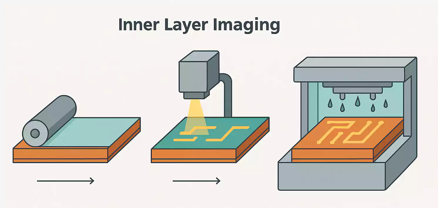
Inner layer imaging is the first step in building the electrical circuitry of a multilayer PCB. It involves transferring the circuit pattern onto copper-clad laminates that will form the board's inner layers. With increasing demand for finer line widths and tighter spacing, manufacturers now prefer Laser Direct Imaging (LDI) over traditional phototools for higher precision and alignment accuracy.
This step is critical for defining the core signal paths, power and ground planes, and high-speed traces that will later be sandwiched during lamination.
1.Photoresist Application
A thin layer of light-sensitive film (photoresist) is laminated onto the cleaned copper surface of the core. This photoresist reacts to ultraviolet (UV) light or laser exposure, allowing selective patterning of the copper layer.
2.Exposure – Laser Direct Imaging (LDI)
Instead of using physical masks, LDI exposes the pattern directly onto the panel using a focused UV laser.
- LDI offers sub-25µm resolution, ideal for HDI and high-frequency designs.
- It eliminates issues related to film shrinkage or misalignment in traditional mask-based imaging.
3.Development and Drying
After exposure, the unexposed (unhardened) photoresist is removed in an alkaline developer. This leaves behind a hardened resist image that protects the desired copper traces during etching.
4.Automatic Optical Inspection (AOI) (often done post-development)
Before proceeding to etching, the imaged inner layers undergo AOI to verify that all traces, pads, and clearances match the original design data (netlist). This helps catch imaging defects early and reduces scrap.
Etching & Photoresist Stripping
Etching is a critical step in defining the conductive circuitry on a PCB’s inner layers. After imaging, the exposed copper areas—those not protected by hardened photoresist—must be removed with high precision to form clean, electrically isolated traces and pads.
This process is typically carried out in a conveyorized etching line that includes etch, strip, rinse, and drying stages, optimized for throughput and consistency.
1.Chemical Etching
The panel is passed through an etching chamber, where it is sprayed with a controlled solution—commonly ammoniacal cupric chloride or ferric chloride—that removes the unprotected copper.
- Etch uniformity is critical for trace width control and impedance performance.
- Over-etching can lead to trace thinning and open circuits; under-etching risks shorts and residual copper.
2.Etch Process Parameters
To ensure repeatable and high-quality results, manufacturers tightly regulate:
- Etchant composition and pH levels
- Panel speed and dwell time
- Spray pressure and nozzle geometry
These parameters are continuously monitored by inline sensors to maintain chemical balance and prevent defects.
3.Photoresist Stripping
Once etching is complete, the hardened photoresist that protected the circuit pattern is no longer needed. It is stripped using a mild alkaline solution in a separate chamber.
- The panel is then rinsed and dried to prepare for optical inspection or lamination.
4.Post-Etch Inspection
AOI (Automated Optical Inspection) is commonly performed at this stage to detect:
- Over-etched or broken traces
- Etch residues or copper slivers
- Pattern misalignment
This ensures any etching anomalies are identified before the board proceeds to the next layer stack-up.
Layer Lamination
Lamination is the process of bonding multiple copper-clad layers together to form a solid, multilayer printed circuit board (PCB). This step transforms individual inner cores and prepreg sheets into a single unified stack-up, ensuring mechanical stability and proper interlayer connectivity.
Proper lamination is critical for high-reliability PCBs, particularly in multilayer, HDI, or high-speed digital designs where precise dielectric thickness and low signal loss are essential.
Key Steps in the Lamination Process:
Stack-Up Alignment
The inner layers (already imaged and etched) are precisely aligned with layers of prepreg (a resin-impregnated fiberglass material) and outer copper foil.
- Registration pins or optical alignment systems are used to ensure layer-to-layer accuracy.
- A cleanroom environment is often used to prevent particle contamination that can cause delamination or shorts.
Vacuum Press Lamination
The stacked layers are placed in a vacuum lamination press under controlled pressure and temperature.
- Typical parameters: ~180–200°C temperature, 150–300 psi pressure, and 60–90 minutes dwell time.
- The resin in the prepreg softens and flows under heat and pressure, bonding all layers together and filling gaps or voids between copper features.
Cooling and Curing
After pressing, the stack is slowly cooled to solidify the resin and lock the layers in place.
- Controlled cooling prevents internal stress, warping, or misregistration.
Post-Lamination Processing
- Excess resin is trimmed from the edges.
- A quick visual inspection is done to detect obvious defects like layer shifting, blisters, or warpage.
- Some manufacturers also perform X-ray registration verification to confirm internal layer alignment—especially for high-layer-count boards.
Drilling
Drilling is the process of creating precise holes in the laminated PCB stack to enable vertical electrical connections between different layers. These holes—known as vias—are later metallized to form conductive paths, allowing signals to travel between layers in a multilayer PCB.
Modern PCB designs may include multiple types of vias: through-holes, blind vias, buried vias, and microvias, depending on complexity and layer count.
Key Aspects of the Drilling Process:
Drill File Import and Registration
The drilling operation begins with importing the NC drill files generated during the CAM stage. These files specify:
- Hole locations and sizes
- Drill type (mechanical or laser)
- Stack-up layer depth (for blind or buried vias)
Precision registration is crucial to avoid annular ring violations or breakout conditions.
Mechanical Drilling
High-speed spindles (typically 100,000–200,000 RPM) are used to drill:
- Through-holes for plated vias
- Tooling holes and fiducials for alignment
Drill bits are usually tungsten carbide and range in diameter from 0.1 mm to over 6 mm. Drill life and breakage are carefully monitored to maintain edge quality.
Laser Drilling (for HDI and Microvias)
For High Density Interconnect (HDI) boards, CO₂ or UV laser drilling is used to form:
- Microvias (<150 µm diameter)
- Blind vias between adjacent layers
Lasers provide high precision without mechanical stress, ideal for mobile, RF, and fine-pitch applications.
Deburring and Desmearing
Post-drilling, holes are cleaned to remove burrs and resin smear:
- Deburring ensures clean edges for better plating adhesion
- Desmearing removes resin residue using plasma or permanganate solution, exposing clean dielectric and copper surfaces
Drill Quality Control
Inspection is done using:
- X-ray systems to verify via alignment and wall integrity
- AOI and sample cross-sectioning to ensure hole cleanliness and dimensional accuracy
Defective holes are flagged for redrilling or panel rejection to ensure downstream plating reliability.
Metallization & Copper Plating
After drilling, the PCB enters the metallization phase, where the freshly created hole walls are made electrically conductive. This step is essential for establishing interlayer connectivity through plated through-holes (PTHs) or vias. Once a conductive path is established, electrolytic copper plating is applied to build up copper thickness on both the hole walls and panel surface.
This dual-stage process ensures structural reliability and robust electrical performance—especially in multilayer and high-density designs.
1.Hole Wall Activation (Electroless Copper Deposition)
The first step involves creating a thin, continuous conductive layer (~0.3–0.5 μm) on the insulating walls of the drilled holes:
- The panel is cleaned and micro-etched to roughen the surface.
- A palladium-based catalyst is applied to initiate autocatalytic copper deposition.
- Electroless copper is deposited uniformly across all surfaces, including the hole walls, enabling subsequent electroplating.
2.Panel Plating (Electrolytic Copper Plating)
Once the hole walls are conductive, the entire panel is submerged in an electrolytic copper bath:
- Current is applied through external electrodes, causing copper ions to plate onto the hole interiors and outer surface copper.
- Copper thickness builds up to meet design specs (e.g., 20–25 μm in holes, 30–35 μm on surfaces).
- Plating uniformity is managed by controlling current density, solution agitation, and panel spacing.
3.Plating Thickness & Quality Control
Critical plating parameters are monitored continuously:
- Thickness checks via X-ray fluorescence (XRF)
- Uniformity mapping across the panel
- Cross-section sampling to verify hole wall coverage and detect voids or cracks
4.Optional: Pattern Plating (For Outer Layer Imaging)
In some processes (like tent-and-etch), copper plating is applied selectively on circuit patterns defined by a photoresist. In this case, panel plating doubles as a foundation for trace buildup before etching.
Outer Layer Imaging and Etching
Outer layer imaging defines the visible copper circuitry on the top and bottom surfaces of the PCB. This process is similar to inner layer imaging, but it follows copper plating and includes additional control to ensure alignment with drilled vias and plated hole positions.
After imaging, the panels undergo another round of chemical etching—this time to remove excess surface copper and reveal the final circuit patterns.
1.Surface Cleaning & Dry Film Lamination
The panel surface is cleaned with micro-etch and scrub rollers to ensure optimal photoresist adhesion.
A dry film photoresist is laminated over both sides of the panel under heat and pressure, forming a uniform coating that responds to UV light or laser exposure.
2.Exposure & Development
- In Laser Direct Imaging (LDI) or phototool exposure, the panel is patterned with the outer layer circuit design.
- UV light selectively polymerizes the photoresist, hardening the areas meant to protect copper traces.
- Unexposed resist is removed in the development process, exposing copper areas to be etched.
3.Pattern Plating (Optional)
In some processes (like pattern plating), additional copper and tin plating are applied to the exposed trace areas before etching. Tin acts as an etch resist in the next step.
4.Outer Layer Etching
The panel enters a conveyorized etching chamber:
- Chemical etchants remove the exposed copper, leaving only the trace structures protected by resist or tin.
- The etching rate, chemistry, and dwell time are carefully managed to maintain line width and spacing tolerances.
- After etching, resist stripping removes any remaining photoresist, revealing the final copper pattern.
5.Post-Etch Inspection (AOI)
Automated Optical Inspection (AOI) is performed to verify:
- Trace integrity and continuity
- Annular ring alignment at via holes
- Shorts, opens, or over-etched features
Catching defects at this stage helps avoid downstream failures in solder mask or assembly.
Solder Mask Application
Solder mask is a protective coating applied over the finished copper traces—except for pads, vias, and other exposed areas—on the outer layers of the PCB. It prevents solder bridging during assembly, protects copper from oxidation, and enhances electrical insulation.
Key Steps in Solder Mask Application:
1. Cleaning and Surface Preparation
The PCB surface is thoroughly cleaned to remove oxidation, fingerprints, and dust. Any residue can affect mask adhesion or lead to delamination during reflow.
2. Solder Mask Coating
A layer of liquid photoimageable (LPI) solder mask is applied via screen printing, curtain coating, or spray coating. LPI is preferred for its fine resolution and strong adhesion, especially on complex or high-density boards.
3. Pre-baking (Optional)
Some processes include a short thermal pre-bake to remove solvents and partially cure the mask, ensuring better imaging accuracy.
4. Exposure and Development
Using phototools or Laser Direct Imaging (LDI), UV light selectively exposes the solder mask to define openings over pads, vias, and test points. Unexposed areas are then washed away in the developer, revealing only the copper to be soldered.
5. Final Curing
The board undergoes a high-temperature bake (typically 150–160°C) to fully cure the solder mask, making it chemically and mechanically robust.
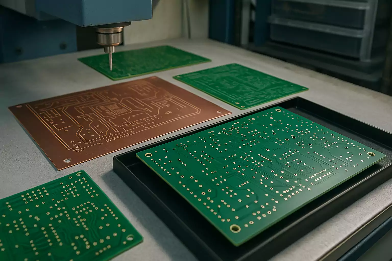
Surface Finish
Surface finish is a critical coating applied to exposed copper pads on the PCB to preserve solderability and protect against oxidation. It ensures a reliable bond during component assembly and contributes to long-term electrical performance.
Common Surface Finishes
1. HASL (Hot Air Solder Leveling)
Molten solder is applied to the board, then leveled using high-pressure air knives.
- Available in leaded and RoHS-compliant lead-free versions.
- Cost-effective and widely used but may not be suitable for fine-pitch components due to uneven surfaces.
2. ENIG (Electroless Nickel Immersion Gold)
A thin layer of gold is plated over a barrier layer of nickel.
- Provides excellent flatness, corrosion resistance, and shelf life.
- Ideal for BGAs, fine-pitch components, and high-reliability applications.
- More expensive than HASL.
3. OSP (Organic Solderability Preservative)
A thin organic layer protects copper pads during storage and assembly.
- Eco-friendly, cost-efficient, and easy to process.
- Best suited for single reflow cycles; not ideal for multiple heat exposures.
4. Immersion Silver and Immersion Tin
These finishes offer flat surfaces and good solderability.
- Immersion silver is common in RF applications due to signal integrity benefits.
- Immersion tin provides good solder joint strength but has shorter shelf life.
Silkscreen (Legend)
Silkscreen, also known as legend printing, is the process of applying text and symbols onto the PCB surface. It provides essential information for assembly, testing, and servicing, including component labels, polarity markers, revision codes, and logos.
Key Aspects of the Silkscreen Process
1. Ink Application Methods
Silkscreen can be applied using:
- Screen printing – the traditional method using stencils; suitable for low-volume or less detailed designs.
- Liquid Photo-Imageable (LPI) ink – provides finer resolution and better adhesion; often used with LDI systems.
- Inkjet printing – ideal for high-resolution, small-font legends and automated workflows.
2. Ink Material and Color
- Typically, white epoxy ink is used for dark solder masks and black or yellow for lighter ones.
- The ink must be heat-resistant to endure reflow and compatible with solder mask materials.
3. Placement and Design Guidelines
- Legends should avoid pads, vias, and solderable surfaces to prevent contamination during assembly.
- Fonts must be legible after solder mask and surface finish application—usually ≥0.8 mm height and 0.15 mm stroke width.
4. Curing and Inspection
- After printing, the board is cured in an oven to harden the ink.
- Visual checks ensure clarity, alignment, and absence of smudging or ink bleed.
AOI & Electrical Test
After all fabrication steps are complete, the PCB undergoes Automated Optical Inspection (AOI) and Electrical Testing (E-Test) to verify structural and functional integrity before shipment. These tests are essential for catching manufacturing defects and ensuring that every board meets design and quality standards.
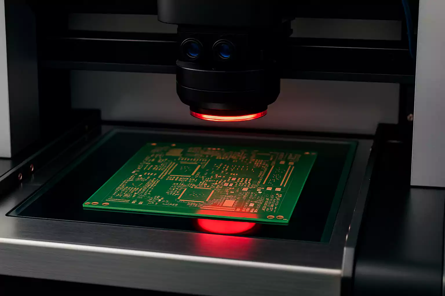
Automated Optical Inspection (AOI)
AOI systems use high-resolution cameras to scan the board’s surface and compare it to the original design files. They detect a wide range of visual defects, including:
- Open circuits or short circuits
- Missing, over-etched, or under-etched traces
- Misaligned vias and silkscreen
- Solder mask misregistration or slivers
AOI is performed at multiple stages, including after imaging, etching, solder mask, and final finish. It provides non-contact, high-speed inspection for 2D features and improves first-pass yield.
Electrical Test (E-Test)
E-Test verifies the electrical continuity of all nets and ensures that no unintended connections (shorts) exist between them. There are two primary methods:
- Flying probe test – uses moving probes to contact test points one by one; ideal for prototypes or small batches.
- Bed-of-nails fixture test – uses a custom fixture with spring-loaded pins to contact all nets simultaneously; best for high-volume production.
These tests confirm:
- All nets are connected as per the netlist
- Vias and plated through-holes are conductive
- There are no shorts between adjacent traces or layers
Routing, V-Scoring & Final Profiling
Once the PCB passes inspection and electrical testing, the final step in fabrication is to separate individual boards from the manufacturing panel. This is done through routing, V-scoring, or a combination of both, depending on the board design and assembly method.
PCB Routing
Routing uses CNC-controlled mechanical mills to cut along the board's outline, forming precise shapes, cutouts, and slots.
- Suitable for complex board geometries or irregular contours
- Leaves small breakout tabs with perforations (mouse bites) to hold the board in the panel for transport
- Tab removal and edge finishing are performed after depanelization
V-Scoring
V-scoring involves creating V-shaped grooves along the top and bottom of the board surface using specialized blades.
- Typically used for rectangular boards with straight edges
- Boards remain attached in a scored panel and are snapped apart during or after assembly
- Depth is carefully controlled (usually 1/3 board thickness from each side) to maintain structural integrity
Edge Finishing and Quality Control
After depanelization:
- Edges are deburred and smoothed to remove sharp corners or burrs
- Dimensions and outline tolerances are verified against Gerber data
- Visual inspection confirms clean profiling and damage-free surfaces
Packing & Delivery
Once final profiling is complete, the finished PCBs are cleaned, packaged, and prepared for shipment. Proper packaging ensures that boards arrive at the customer’s location free from contamination, warping, or mechanical damage.
Cleaning and Final Inspection
Before packing, PCBs are thoroughly cleaned to remove any remaining dust, fingerprints, or flux residues. A final visual and dimensional inspection is performed to confirm:
- Board count matches the order
- No scratches, warping, or cosmetic defects
- Surface finish and silkscreen are intact and legible
ESD-Safe and Moisture-Resistant Packaging
To protect against environmental damage:
- PCBs are vacuum-sealed or wrapped in anti-static bags to prevent electrostatic discharge (ESD)
- Moisture barrier bags (MBBs) may be used for sensitive finishes like ENIG or immersion silver
- Desiccant packs and humidity indicators are added when necessary to maintain shelf life
Labeling and Documentation
Each shipment includes clear labeling for easy traceability:
- Job number, part number, quantity, and revision level
- Lot/date code and RoHS/lead-free compliance status
- Optional certificates: C of C, electrical test report, and inspection summary
Shipping and Logistics
Boards are packed in foam-padded cartons or rigid trays to avoid bending and vibration during transit.
Fast-turn services often include:
- Same-day dispatch for prototypes
- Worldwide express shipping with tracking
- Custom packaging options for consignment or turnkey assembly
Quality Control & Troubleshooting
Effective quality control ensures that every PCB meets performance, reliability, and regulatory standards. It spans the entire production process—from imaging to final inspection.
In-Line Quality Control
At each critical step:
- AOI checks trace and pad accuracy
- Plating and etching are monitored for uniformity
- Drilling is inspected for via alignment and burr-free holes
- Solder mask and silkscreen undergo visual and positional checks
Processes follow IPC-6012 guidelines, with traceability maintained via barcodes or lot codes.
Final Testing
Before delivery:
- Cross-section analysis confirms copper thickness and bonding
- Electrical test ensures all nets are open-free and short-free
- Warp/twist checks validate mechanical stability
- Visual inspection ensures cosmetic and dimensional compliance
Common Issues & Solutions
| Issue | Root Cause | Prevention |
|---|---|---|
| Delamination | Moisture, press profile errors | Pre-bake materials, optimize lamination |
| Plating voids | Incomplete hole activation | Improve desmear and chemical prep |
| Trace defects | Etch undercut, imaging shifts | Tighten process control, AOI |
| Solder mask offset | Shrinkage, misalignment | Use LDI, calibrate exposure |
| Warpage | Uneven cooling or material mismatch | Control lamination and cool-down |
Summary: From Design to Deliverable
PCB manufacturing is a complex, multi-stage process that transforms digital circuit designs into high-performance physical boards. Each step—from pre-production engineering to final inspection—must be executed with precision to ensure electrical functionality, mechanical integrity, and manufacturability.
By understanding every stage—imaging, etching, drilling, plating, solder masking, surface finishing, testing, and profiling—designers and engineers can make better decisions, reduce production issues, and optimize designs for both cost and reliability.
A strong partnership with an experienced PCB fabricator is key to achieving consistent quality, fast lead times, and compliance with evolving industry standards.
