


In the world of electronics manufacturing, the term "flip board PCB" can refer to two very different things. Some engineers use it when talking about flip-chip packaging technology and its integration with PCB designs. Others mean literally flipping or mirroring a PCB layout in their EDA software. This comprehensive guide covers both interpretations, delivering actionable insights, best practices, and expert-level checklists. Whether you're designing a high-density BGA with flip-chip dies or simply trying to mirror a board in KiCad, this guide has you covered.
What Does "Flip Board PCB" Really Mean?
When users search for "flip board PCB," they typically fall into one of two categories:
- Flip-Chip Packaging on PCB: Refers to the use of flip-chip ICs (integrated circuits mounted face-down) directly onto the PCB or an interposer. This approach is common in high-performance, high-density designs such as smartphones, networking equipment, and advanced computing.
- EDA-Based Board Flipping: Involves using software tools like KiCad or EasyEDA to mirror or flip the PCB layout during design or manufacturing prep.
This article addresses both topics, prioritizing flip-chip packaging while also providing practical EDA flipping tips at the end.
Flip-Chip on PCB: Concepts, Benefits, and When to Use
What is Flip-Chip?
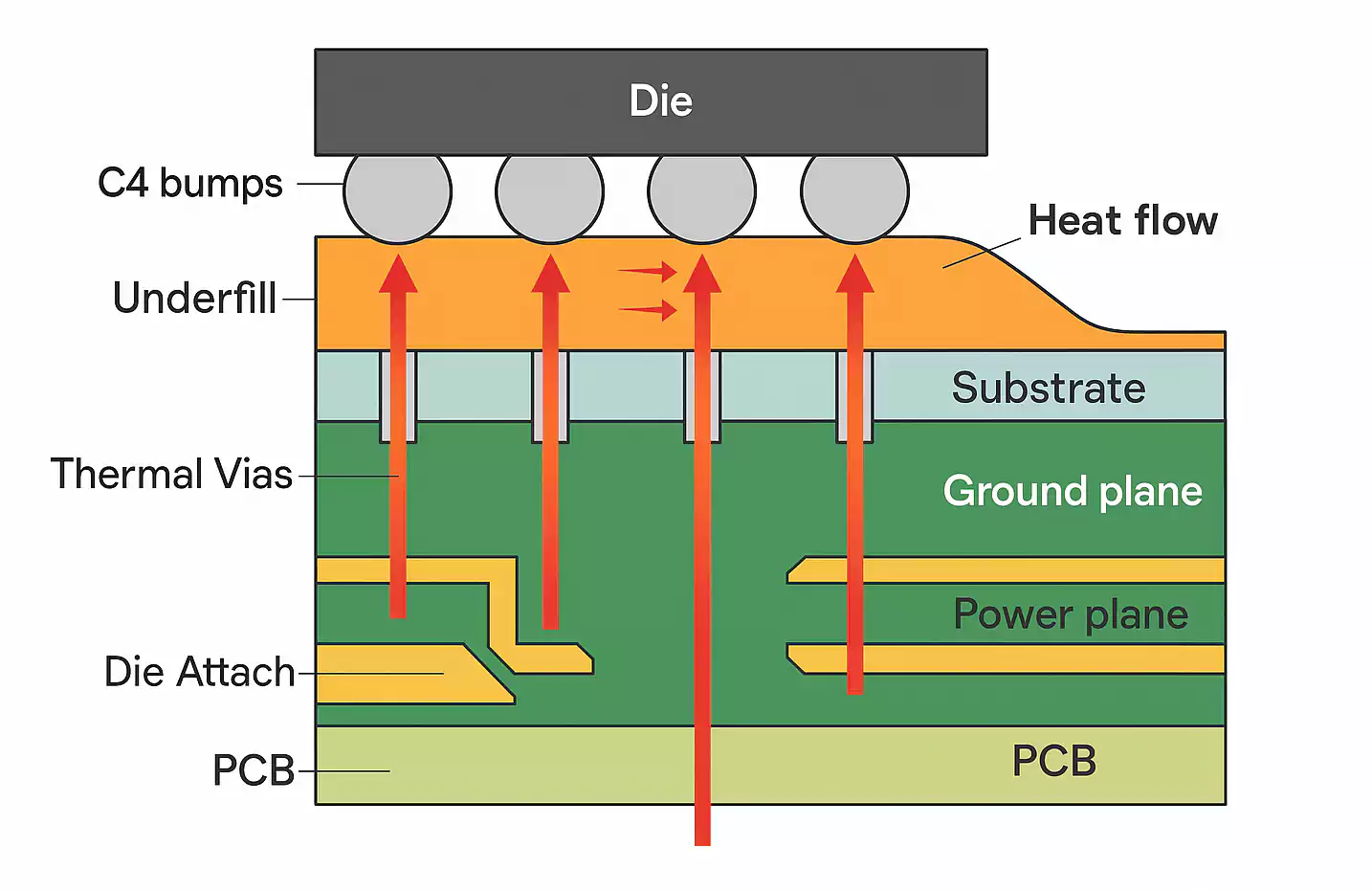
Flip-chip is a semiconductor packaging method where the silicon die is flipped and mounted face-down, allowing direct electrical connection between the die and substrate using solder bumps (also called C4 bumps). Instead of wire bonding, flip-chip provides short, high-density interconnections.
Benefits of Flip-Chip Packaging:
- Electrical Performance: Lower inductance and parasitics due to short interconnect paths.
- Thermal Management: Better heat dissipation through the substrate and die surface.
- Size Efficiency: Enables compact layouts with more I/O per unit area.
Common Use Cases:
- High-speed processors (CPU, GPU)
- RF components
- Advanced BGA and SiP (System-in-Package) designs
- Devices requiring fine pitch and miniaturization
Flip-Chip Assembly Flow on PCB
The typical flip-chip packaging process for PCB integration involves:
- Bump Deposition: The silicon die is fabricated with solder bumps.
- Die Placement: The die is flipped and aligned with the substrate.
- Reflow Soldering: Heat is applied to form permanent joints.
- Underfill Application: Epoxy is dispensed to fill the gap between the die and substrate, improving mechanical strength and reliability.
- Cleaning and Inspection: Excess materials are removed, and joints are inspected via X-ray or AOI.
The underfill is particularly important—it compensates for thermal mismatch and reduces stress on the solder bumps during thermal cycling.
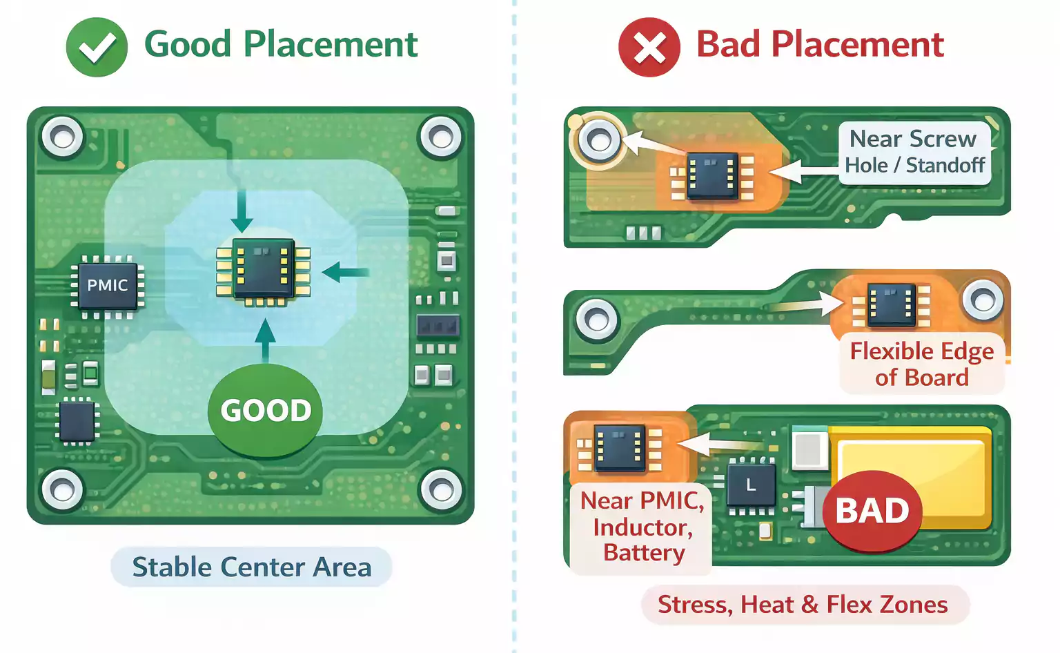
PCB Layout Best Practices for Flip-Chip/FC-BGA
Designing a PCB that integrates flip-chip or FC-BGA components requires precision and attention to layout details. Here are the key best practices:
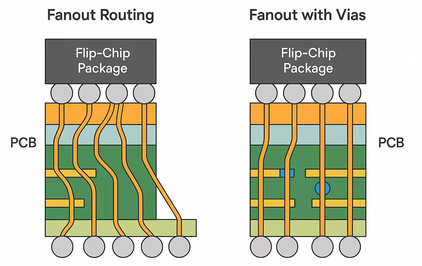
1. Fanout Strategy
- Use via-in-pad or microvia to reduce routing congestion.
- Employ HDI (High-Density Interconnect) stackups to support fine-pitch breakout.
- Avoid long trace lengths from the center die to outer ball pads.
2. Impedance and Signal Integrity
- Maintain consistent reference planes.
- Use differential pair routing and matched trace lengths for high-speed signals.
- Consider return paths and minimize stubs.
3. Power and Ground Planning
- Provide low-impedance power distribution with solid planes.
- Place decoupling capacitors close to power balls.
- Use multiple vias to minimize ESL/ESR in critical nets.
4. Thermal Design
- Increase copper thickness or area for heat dissipation.
- Utilize thermal vias to transfer heat to inner or bottom layers.
- Simulate thermal behavior if power exceeds 1–2 W/cm².
5. Material and Stackup Considerations
- Choose substrates with low CTE mismatch (e.g., BT, ABF).
- Balance layer count vs. routability.
- Ensure Dk/Df consistency for controlled impedance.
6. Footprint and Land Pattern
- Verify land pattern from manufacturer datasheet.
- Use IPC-7351 compliant libraries.
- Ensure accurate alignment for reflow profiles.
Flip-Chip vs. Wire-Bond vs. BGA: Decision Matrix
| Feature | Flip-Chip | Wire-Bond | BGA |
|---|---|---|---|
| Electrical Performance | Excellent | Moderate | Good |
| Thermal Dissipation | High | Low | Medium |
| Package Size | Very Compact | Larger | Compact |
| Assembly Complexity | High | Low | Medium |
| Cost | Higher | Lower | Medium |
| Application | High-end, RF, miniaturized | Low-cost ICs | General use |
When to use Flip-Chip:
- High-performance computing
- Fine-pitch or I/O-dense applications
- Thermal-critical designs
DFM/DFX Checklist for Manufacturing Success
To ensure the successful fabrication and assembly of flip-chip designs:
1.Design for Manufacturability (DFM):
- Confirm minimum trace width/spacing per vendor.
- Align pad sizes with stencil and bump dimensions.
- Avoid non-standard pad shapes unless required.
2.Design for Assembly (DFA):
- Use fiducials and global/local markers for alignment.
- Document underfill type and process parameters.
- Provide assembly drawing and reflow profile.
3.Design for Testability (DFT):
- Add test points for JTAG/functional validation.
- Allow for boundary scan access if possible.
4.Deliverables:
- Gerber or ODB++
- BOM with clear part numbers and alternatives
- Pick-and-Place file with exact coordinates
- Stackup drawing with impedance details
Troubleshooting & Reliability Concerns
Flip-chip assemblies introduce challenges in manufacturing and long-term reliability:
Common Issues:
- Open/shorted bumps
- Voids in underfill
- Warping of the die or PCB
- Inadequate cleaning under the die
Inspection Tools:
- 2D/3D X-ray
- Scanning Acoustic Microscopy (SAM)
- Automated Optical Inspection (AOI)
Reliability testing (thermal cycling, vibration, moisture sensitivity) is essential for high-stress environments.
How to "Flip" a PCB in EDA Tools (Secondary Intent)
While "flip board PCB" usually refers to flip-chip, some users simply want to flip their board layout in CAD software. Here's how:
KiCad:
- Press
Fto flip a component or board side. - Use
View > Flip Board Viewfor mirror inspection. - Ensure text is mirrored properly when flipping layers.
EasyEDA:
- Right-click and use Flip Horizontally/Vertically.
- Check pad orientation and net continuity after flipping.
- Use Gerber preview to verify mirror accuracy.
Important: Flipping a board for single-sided assembly or stencil production requires both layers and silkscreen to be mirrored—but netlist connections must remain intact.
FAQs
Q1: Is Flip-Chip the same as BGA?
A: No. Flip-chip refers to a die attachment method. BGA is the package form factor. A flip-chip can be used inside a BGA.
Q2: Do all Flip-Chip PCBs require underfill?
A: Most high-reliability or thermal-stress applications use underfill, but it's optional in low-stress environments.
Q3: Is Flip-Chip always more expensive?
A: Not always. For high-density, high-performance designs, flip-chip technology may reduce the number of board layers or size, thereby offsetting the cost.
Q4: Can I use standard PCB materials with Flip-Chip?
A: Only if the CTE and thermal properties match. Specialized materials (like ABF) are often required.
Summary and Takeaways
Flip-chip technology offers unparalleled performance for modern electronics, but it also introduces layout and manufacturing complexity. With careful planning, collaboration with manufacturers, and adherence to DFM/DFX principles, flip-chip PCBs can provide thermal, electrical, and space-saving benefits.
Meanwhile, for those using "flip board PCB" to refer to EDA tricks, understanding how to mirror designs properly ensures accurate manufacturing output.
