Introduction & Background
In today’s fast-paced electronics industry, devices are getting smaller, lighter, and more complex. From smartwatches and wearable medical sensors to compact aerospace systems, the demand for flexible, space-saving designs is reshaping how circuits are built.
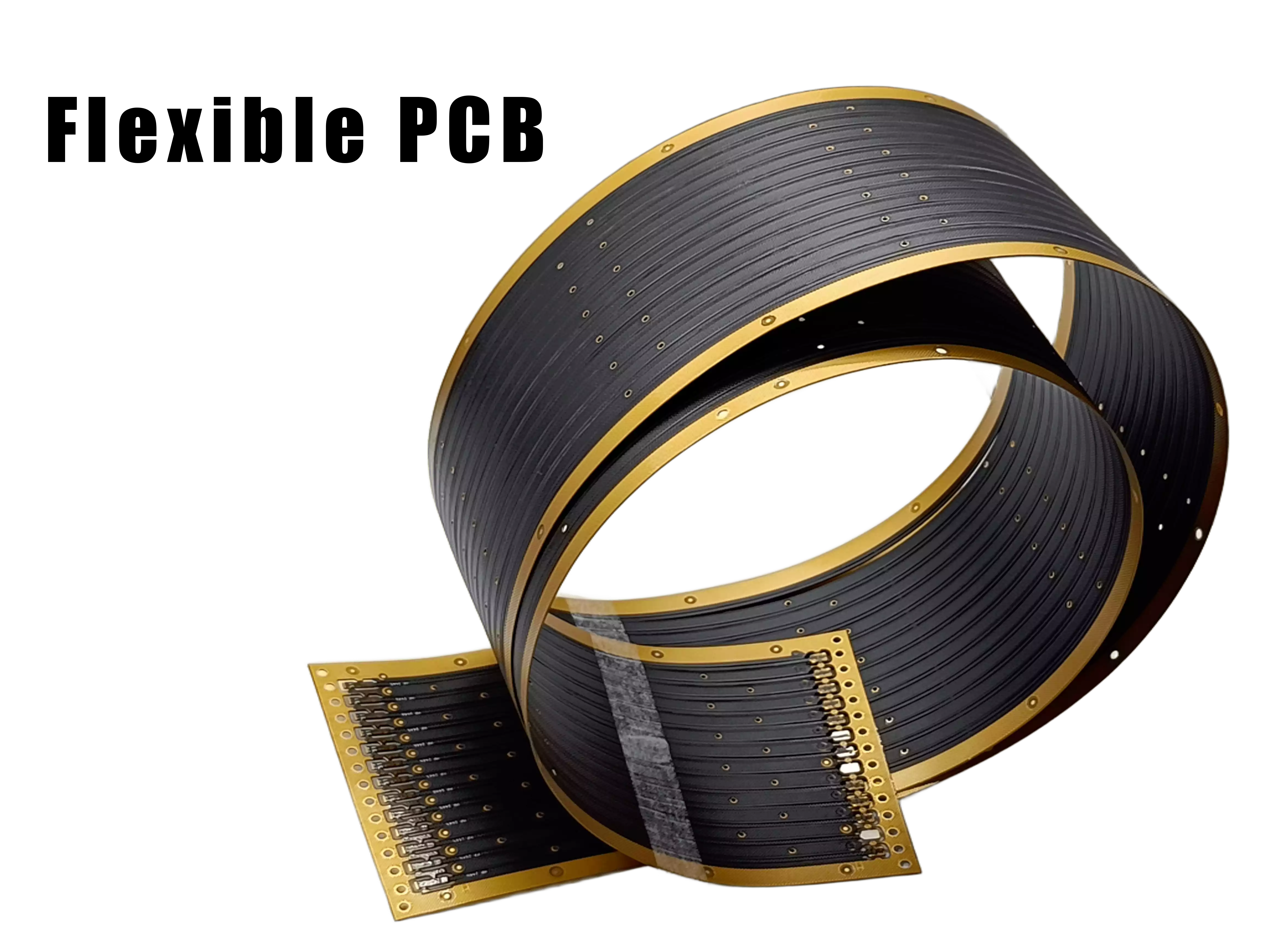
That’s where flexible PCBs, or flex PCBs, come in. These bendable circuit boards are engineered to fit into tight, irregular spaces where traditional rigid boards fall short.
So why the growing shift toward flex? It's all about maximizing function while minimizing bulk. Flex PCBs offer unique advantages: they’re thin, they can twist and bend without breaking, and they enable 3D circuit design, opening the door to more compact and creative hardware.
But there’s a trade-off—flex PCBs are more complex and typically more expensive than their rigid counterparts. That’s why smart engineers don’t just ask "Can we use flex?"—they ask "Should we?"
What Exactly Is a Flex PCB?
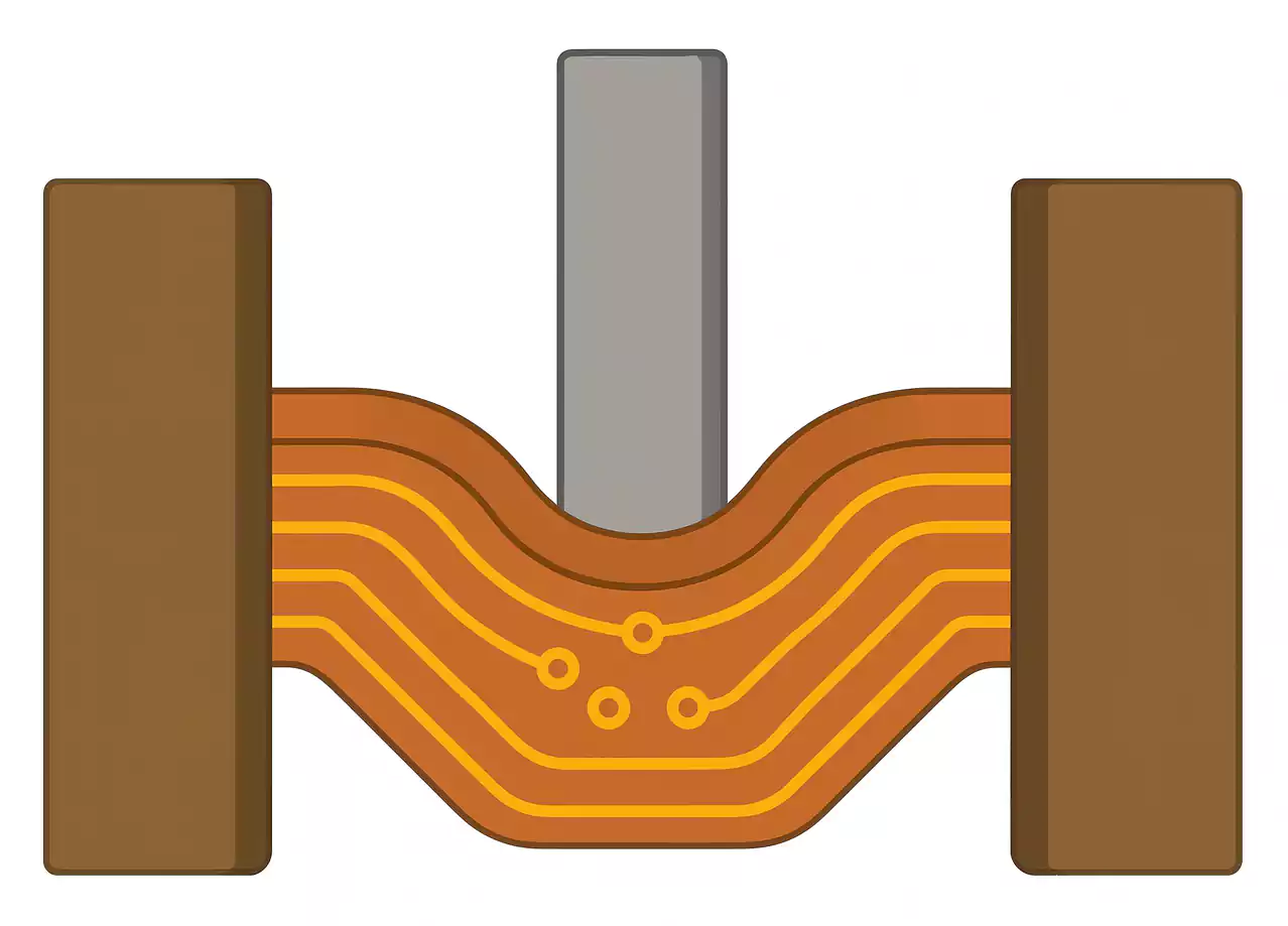
A flex PCB (flexible printed circuit board) is a circuit built on a flexible polyimide or polyester substrate instead of a rigid FR4 base. It allows electrical connections to be routed through bending or curved mechanical structures without compromising signal integrity or structural reliability.
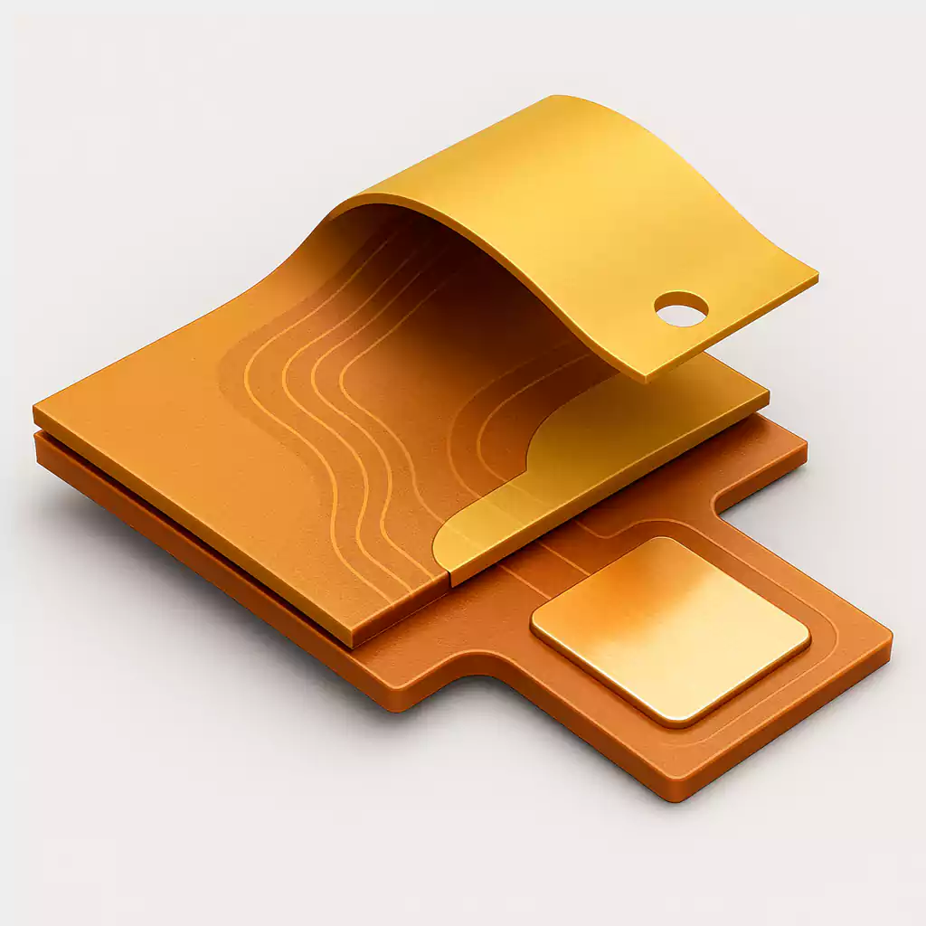
Structurally, a flex PCB consists of one or more layers of etched copper traces laminated onto the flexible base, protected by a coverlay or flexible soldermask. These circuits are designed to maintain performance under mechanical stress such as folding, vibration, or repeated motion.
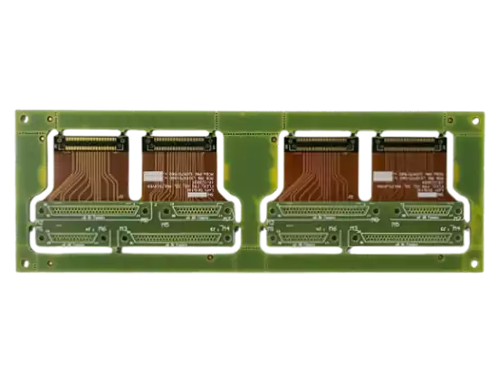
Flex PCBs are often used in areas where space constraints, weight reduction, or dynamic flexing are critical. They can be used alone or in combination with rigid sections as part of a rigid-flex assembly
The Main Types of Flex PCBs
1.Single-Sided Flex PCB
A single conductive layer on a flexible substrate, typically polyimide. Components and traces are placed on one side only.
Features: Lightweight, highly flexible, and low cost
Applications: LED strips, printers, simple connectors
2.Double-Sided Flex PCB
Conductive layers on both sides of the substrate, interconnected with plated through-holes (PTH).
Features: Increased circuit density, moderate flexibility
Applications: Wearable devices, compact sensors
3.Multilayer Flex PCB
Three or more conductive layers laminated with insulating films. Vias connect layers to support complex routing.
Features: High-density interconnects, controlled impedance, suitable for dynamic bending zones
Applications: Smartphones, cameras, medical electronics
4.Rigid-Flex PCB
Combines flexible and rigid sections in one structure. The flexible areas handle dynamic bending, while rigid parts offer mechanical support and ease of assembly.
Features: Space-saving, reduced interconnects, improved reliability
Applications: Aerospace, medical implants, foldable electronics, automotive modules
Design Tips for Flex PCBs
1.Material Selection & Thickness
Use polyimide for flexibility and thermal stability.
Choose RA (rolled annealed) copper for dynamic bending; avoid ED copper in high-flex zones.
Thinner materials improve flexibility but may require reinforcement.
2.Bend Radius & Flex Life
Static bend: Minimum radius ≈ 6× board thickness
Dynamic bend: Minimum radius ≥ 12× thickness
Tighter bends reduce lifespan.
3.Trace Routing & Copper Tradeoffs
Use smooth curves—avoid sharp angles.
Route perpendicular to bend axis when possible.
Thin copper (≤0.5 oz) reduces stress in flex areas.
Avoid traces over stiffeners, holes, or slots.
4.Coverlay vs. Silkscreen
Coverlay (polyimide + adhesive) protects traces in bend zones.
Silkscreen is for labeling only—not for mechanical protection.
5.Stiffeners: Purpose & Placement
Add under connectors, components, or mounting holes.
Use FR-4, polyimide, or stainless steel as needed.
Prevent over-bending and improve assembly stability.
6.Mechanical Reliability Enhancements
Use teardrops for pad-to-trace transitions.
Avoid vias in bend regions.
Apply strain relief patterns in high-stress areas.
Anchor pads properly to reduce delamination risk.
Reliability & Real-World Challenges of Flex PCBs
1.Mechanical and Thermal Stress
Repeated bending, vibration, and assembly-related flexing can cause:
- Cracked traces, especially near sharp bends or corners
- Delamination between copper, adhesive, and coverlay layers
- Pad lifting from insufficient anchoring
Maintain proper bend radius, use rounded traces, and avoid placing vias or components in flex zones.
2.Surface Finishes and Solderability
Surface finish affects both assembly quality and field reliability.
- ENIG: Durable, suitable for fine-pitch components
- OSP: Cost-effective, but limited shelf life
- Immersion silver or tin: Balanced choice, sensitive to handling
3.Environmental Factors
- Moisture: Can lead to corrosion or dielectric failure
- Chemicals: May degrade adhesives and coverlays
- Sulfur: Tarnishes silver finishes—use sulfur-free storage materials
4.Connector Zones and Reinforcement
Stress concentration near connectors or soldered interfaces is a common failure point.
- Use stiffeners under connectors to prevent bending stress
- Avoid routing traces through rigid-to-flex transition areas
- Apply strain relief in layout and enclosure design
Applications of Flex PCBs
Flex PCBs are widely adopted across industries thanks to their lightweight design, mechanical flexibility, and ability to support compact, high-density circuits.
Consumer Electronics
Used in lightweight, space-constrained devices such as smartwatches, fitness bands, foldable phones, and wireless earbuds. Enables compact layouts and high signal integrity for wearable and portable tech.
Automotive Systems
Supports flexible interconnects between sensors and ECUs in ADAS, dashboards, infotainment units, and LED lighting. Flex PCBs help reduce wiring complexity while withstanding vibration and thermal cycles.
Medical Devices
Ideal for small, biocompatible electronics including wearable health monitors, hearing aids, and imaging tools like endoscopes. Offers reliable connections in compact and irregular-shaped enclosures.
Industrial Automation
Applied in robotic arms, compact sensor modules, and moving machinery parts. Flex circuits increase system reliability by eliminating bulky connectors and improving vibration resistance in motion-heavy systems
When to Use Flex vs Rigid-Flex PCBs
Flex PCB
Use when:
- Only the interconnect area needs flexibility
- Minimal mechanical stress or bending cycles
- Space and weight constraints exist
- Lower cost and simpler structure are priorities
Rigid-Flex PCB
Use when:
- Both flexible routing and rigid support are required
- The design involves frequent bending, vibration, or dynamic stress
- Connector reliability and long-term durability are critical
- Integration and space optimization are needed in 3D assemblie
Understanding Flex PCB Bend Radius
The safe bend radius of a flex PCB is usually calculated as:
Minimum Bend Radius = 10 × T
(where T is the total thickness of the flex material)
For example, a 0.1 mm thick flex circuit should not be bent tighter than a 1 mm radius. Going beyond this could crack copper traces or delaminate layers.
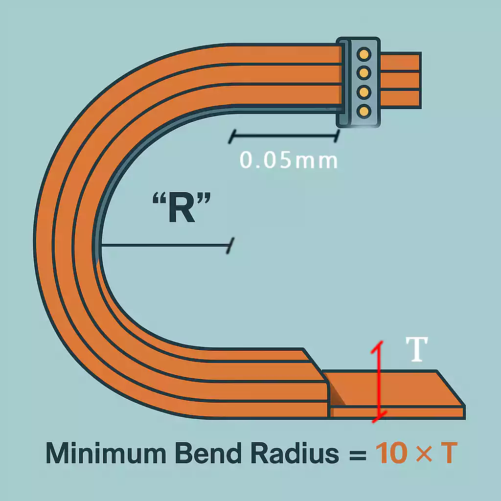
As the image illustrates, plating through-holes or placing components near bend zones should be avoided—especially when performing sharp bends like 90° or tighter. Excessive bending can weaken solder joints and lead to early failure
In some cases, 180-degree folds are possible, but only when using ultra-thin, single-layer flex materials specifically designed for dynamic applications.

Conclusion
Flexible PCBs enable lighter, smaller, and more reliable designs across industries. Their mechanical flexibility and electrical performance make them ideal for compact, high-density applications. As design demands evolve, flex PCBs will remain a preferred choice for advanced electronic systems