


Introduction
Printed Circuit Boards (PCBs) provide structural support and electrical pathways in electronic devices. When a trace breaks or an PCB Open Circuit occurs, it can cause malfunction or failure.
Common causes include mechanical stress, heat, electrical overload, or corrosion. Most issues are local and repairable with the right tools and techniques.
This guide offers practical methods to diagnose and fix damaged PCBs efficiently and safely.
You will learn to:
- Identify signs of open circuits and broken traces
- Use diagnostic tools for precise fault detection
- Apply effective, scenario-based repair techniques
- Follow safety best practices throughout the process
Common Fault Types and Causes
Understanding the types of PCB faults is the first step toward effective repair. While there are many possible board failures, two of the most common in PCB repair work are open circuits and broken copper traces.
Open Circuit – Definition and Characteristics
An open circuit occurs when the electrical path between two points is interrupted, preventing current from flowing. In the context of a PCB, this can mean a broken track, a failed solder joint, or even an internal layer break in a multilayer board.
If you want a deeper technical breakdown, see our detailed article on open circuit explained — it covers the principles, testing methods, and real-world examples in more depth.
Key symptoms of an open circuit include:
- A complete lack of signal or power on certain sections of the board.
- Intermittent operation when the board is flexed or tapped.
- Higher-than-expected resistance readings between connected points.
Broken Copper Trace
A broken copper trace is a physical discontinuity in the conductive pathway of a PCB. This can occur on the surface layer where it’s visible, or in inner layers of a multilayer PCB where it is more challenging to detect. Surface trace breaks are often identifiable as fine cracks, burnt spots, or missing copper foil.
Common Causes of Open Circuits and Broken Traces
PCB open circuits and broken traces can result from:
- Mechanical Stress – Excessive bending, vibration, or accidental drops can crack copper traces or fracture solder joints.
- Thermal Damage – Overheating due to component failure or excessive soldering temperature can cause copper to lift or burn.
- Electrical Overload – High current surges may vaporize sections of a trace, leaving a gap.
- Chemical Corrosion – Moisture, flux residue, or exposure to harsh chemicals can slowly degrade copper over time.
- Manufacturing Defects – Poor soldering, insufficient copper thickness, or improper lamination can create weak points that fail prematurely.
How to Identify an Open Circuit or Broken Trace
Visual Inspection
Start with a careful visual inspection — it’s the quickest way to spot obvious problems before breaking out test equipment.
- Magnification Tools: Use a loupe or digital microscope to inspect traces, pads, and solder joints for cracks, burns, or lifted copper.
- Lighting Technique: Shine a bright light at a shallow angle across the PCB surface to highlight tiny discontinuities or trace damage.
- Signs to Look For: Hairline fractures in copper, discolored areas indicating heat damage, or missing segments of the trace.

Continuity Testing with a Multimeter
A multimeter in continuity mode is one of the most effective tools for detecting open circuits and broken traces.
Steps:
- Disconnect all power from the board.
- Place the probes at two points along the same trace or circuit path.
- If the multimeter beeps (low resistance), the path is intact; no beep indicates an open circuit.
Advantages:
- Quick and reliable for surface-level faults.
- Can confirm suspected damage spotted during visual inspection.
Signal Tracing with an Oscilloscope or Signal Injector
For more complex boards or intermittent faults, an oscilloscope or signal injector can help.
- Inject a known waveform at one end of the suspected trace.
- Use the oscilloscope to measure along the trace until the signal disappears — the break point is between the last good reading and the first bad reading.
This is especially useful for high-frequency signal lines where continuity testing may not reveal partial breaks or impedance changes.
Thermal Imaging for Indirect Detection
A thermal camera or infrared thermometer can sometimes locate open circuits indirectly.
- An open trace in a power circuit may cause nearby components to overheat or remain cooler than expected.
- Comparing thermal patterns against a known-good board can reveal anomalies.
Using Reference Schematics and Layout FilesIf available, schematics and PCB layout files make fault detection faster.
- Match probe points to net labels to ensure you are testing the correct connections.
- Identify possible alternate test points for traces that are not directly accessible.
Safety Precautions and Tools Needed Before Repair
Before you start repairing a PCB open circuit or broken copper trace, it’s critical to follow proper safety procedures and have the right tools on hand.
Safety Precaution
1. Disconnect Power Completely
Always disconnect all power sources before touching the PCB. Even a seemingly harmless low-voltage circuit can store dangerous energy in capacitors. In high-voltage equipment, failing to discharge capacitors properly can result in electric shock.
2. Discharge Capacitors
Use a resistor or a dedicated discharge tool to safely release stored energy in capacitors. Never short a capacitor with a screwdriver — it’s dangerous and can damage components.
3. Electrostatic Discharge (ESD) Protection
Static electricity can silently destroy sensitive components. Wear an ESD wrist strap, use an anti-static mat, and ensure your work area is properly grounded.
4. Ventilation and Fume Safety
Soldering produces fumes that contain flux residues. Work in a well-ventilated space or use a fume extractor to protect your lungs.
5. Fire Safety
Keep a small electronics-rated fire extinguisher nearby. Soldering irons and hot-air stations can ignite flammable materials if left unattended.
Essential Tools for PCB Repair
To repair open circuits and broken traces efficiently, you’ll need a set of specialized tools and materials.
Basic Hand Tools
- Soldering Iron (temperature-controlled, fine tip for precision work)
- Hot Air Rework Station (for removing or reflowing components)
- Tweezers (ESD-safe for handling small parts)
- Precision Wire Cutters and Strippers
Diagnostic Equipment
- Digital Multimeter (with continuity mode and low-resistance measurement)
- Oscilloscope (for signal tracing and waveform analysis)
- Magnification Tools (loupe or microscope for close inspection)
Repair Materials
- Fine-Gauge Wire (e.g., 30AWG wire-wrap or enamel-coated magnet wire for jumper repairs)
- Solder and Flux (lead-free or leaded, depending on compliance requirements)
- Kapton Tape (heat-resistant insulation)
- Conductive Silver Ink or Conductive Adhesive (for cold repairs without soldering)
Optional but Helpful
- PCB Holder or Vice (keeps the board stable during repair)
- Thermal Camera (for indirect fault detection and verification after repair)
- Alcohol and Cleaning Brushes (to remove flux residues)
PCB Open Circuit and Broken Trace Repair Methods
Once you’ve identified the location of an open circuit or broken copper trace on a PCB, you can choose the most appropriate repair technique based on the severity, location, and accessibility of the fault. Below are the most common and effective repair methods used by both professionals and hobbyists.
Jumper Wire Repair (Fly-Wire Method)
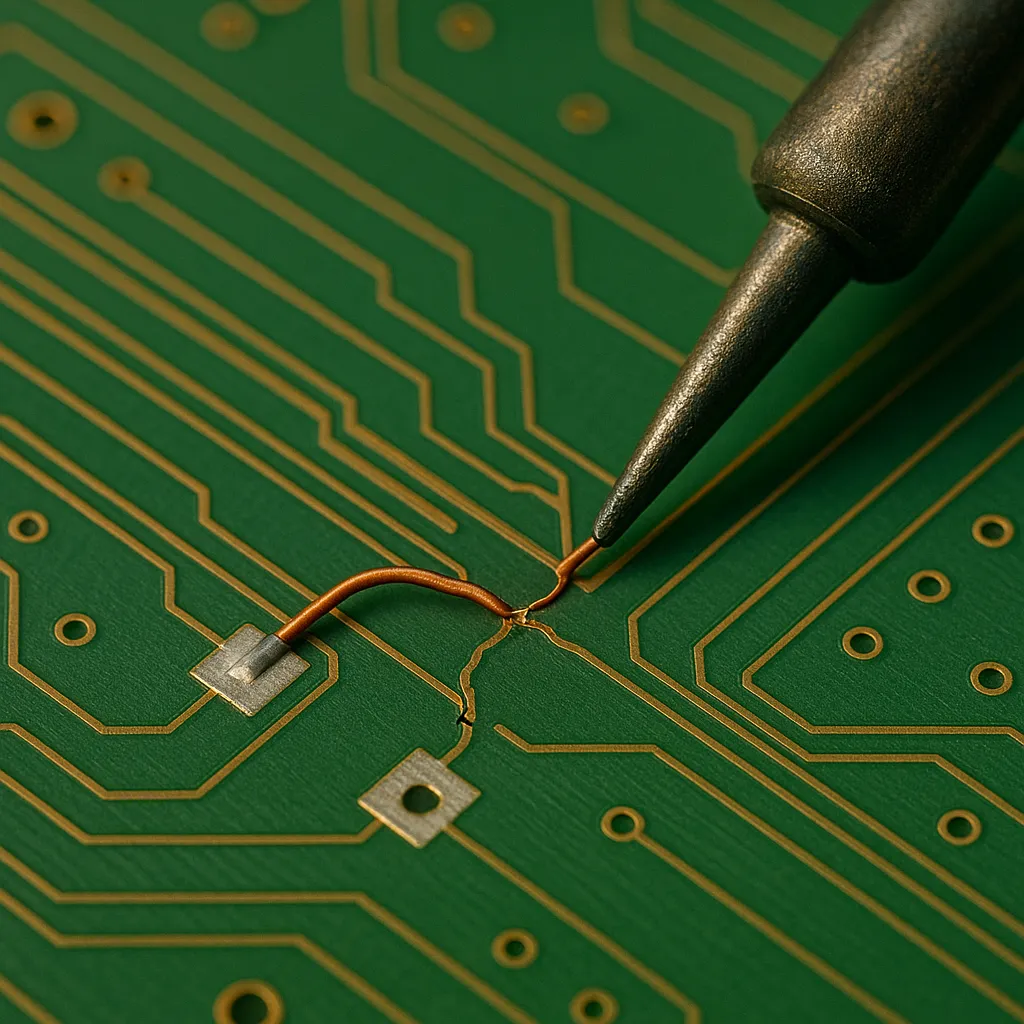
Best For:
- Long breaks in a trace
- Damage to multilayer boards where the internal trace cannot be accessed
- High-current paths that require low-resistance restoration
Materials Needed:
- Fine-gauge insulated wire (30AWG wire-wrap or enamel-coated magnet wire)
- Solder and flux
- Kapton tape or adhesive for securing the wire
Procedure:
- Locate Connection Points – Identify two solderable points at each end of the broken circuit.
- Prepare the Surface – Scrape away a small section of the solder mask to expose copper, or use existing pads/vias.
- Tin the Pads – Apply a thin layer of solder to ensure good adhesion.
- Attach the Wire – Solder one end of the jumper wire to the first pad, route it neatly, and solder the other end to the second pad.
- Secure and Protect – Fix the wire in place with Kapton tape to prevent movement and stress.
Advantages:
- Very reliable and strong
- Suitable for bypassing hidden or inaccessible trace breaks
Limitations:
- Can be less aesthetically pleasing
- Requires good soldering skills for fine-pitch areas
Solder Bridge Repair
Best For:
- Very short breaks in surface traces
- Small copper gaps due to abrasion or burns
Materials Needed:
- Fine-tipped soldering iron
- Flux
- Solder
Procedure:
- Clean the Area – Remove dirt, corrosion, or old solder using isopropyl alcohol.
- Expose the Copper – Gently scrape the solder mask from each side of the break.
- Apply Flux – This helps solder flow and adhere evenly.
- Create the Bridge – Use the iron to flow solder between the two exposed copper ends, forming a shiny, continuous path.
Advantages:
- Quick and simple
- Minimal additional materials needed
Limitations:
- Not ideal for high-current paths
- Risk of creating unintended shorts if solder spreads too far
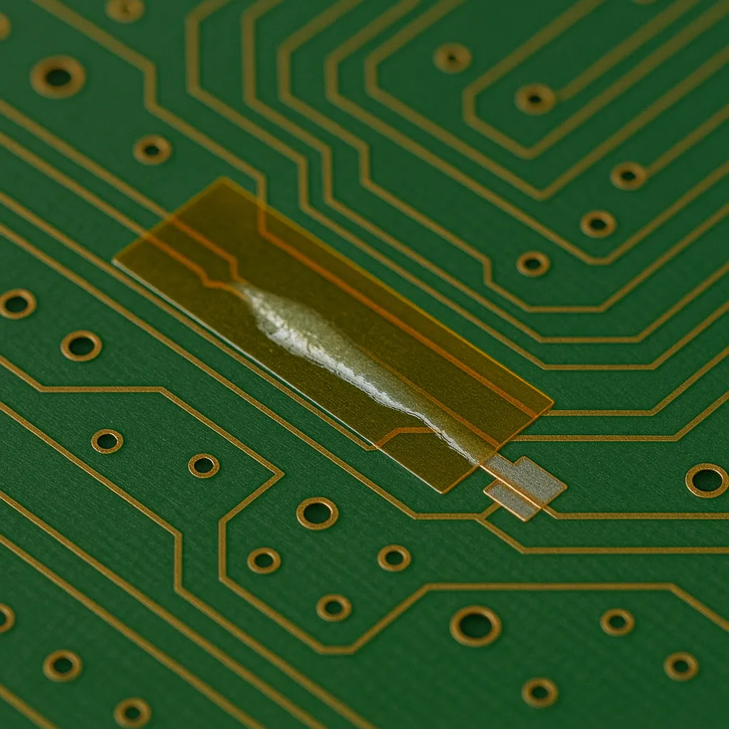
Conductive Ink or Conductive Adhesive
Best For:
- Heat-sensitive PCBs or components
- Situations where soldering is impractical or risky
Materials Needed:
- Conductive silver ink or conductive epoxy adhesive
- Applicator brush or fine needle tip
- Protective coating (optional)
Procedure:
- Clean the Break Area – Ensure no oxidation or dirt remains.
- Apply the Conductive Material – Use a fine applicator to connect the broken trace ends.
- Cure or Dry – Follow the manufacturer’s instructions for drying (may require heat or UV curing).
- Protect – Apply a clear insulating layer for durability.
Advantages:
- No heat required, preventing thermal stress
- Works on delicate or flexible PCBs
Limitations:
- Lower conductivity than copper or solder
- May degrade over time under mechanical stress
Copper Foil Replacement
Best For:
- Large missing copper areas
- Burned or peeled traces
Materials Needed:
- Thin adhesive copper foil tape or cut copper sheet
- Soldering tools or conductive adhesive
- Protective solder mask or epoxy coating
Procedure:
- Cut the Copper Foil – Shape it to match the missing trace segment.
- Attach to PCB – Use the foil’s adhesive backing or apply conductive glue.
- Solder for Conductivity – If soldering, ensure strong electrical and mechanical bonding.
- Protect and Finish – Apply a solder mask or clear coating to protect the repair.
Advantages:
- Restores original copper width for current capacity
- Professional-looking result if done carefully
Limitations:
- Requires precise cutting and alignment
- Adhesives can weaken over time
Multilayer PCB Special Repairs
Challenges:
- Broken traces inside inner layers are not visible or directly accessible
- Standard solder bridge or copper foil repairs are not possible internally
Possible Solutions:
- Jumper Wires – Bypass the internal break by routing a wire on the outer layer.
- Via-to-Via Wiring – Connect accessible vias on each side of the break.
- Component Pin Bridging – Use component pins as intermediate connection points.
Post-Repair Testing and Protection
After repairing a PCB open circuit or broken copper trace, proper testing ensures the fix is reliable and safe. Skipping this step risks damaging the board further or causing recurring failures.
Electrical Testing
1. Continuity Check
Use a digital multimeter in continuity mode to verify that your repair fully restores the electrical path. Test directly between the original trace endpoints — the meter should beep or show near-zero resistance.
2. Resistance Measurement
Switch to resistance mode for a more precise check, especially for high-current traces. The reading should be comparable to an equivalent, undamaged trace on the same board.
3. Power-On Verification
Reconnect power and observe normal device startup. If possible, compare voltage readings at test points to a known-good reference board or schematic.
Functional Testing
1. Component-Level Checks
If the repair was part of a signal or power path, confirm that connected components are functioning properly — LEDs lighting, motors running, or ICs receiving correct power.
2. Stress Testing
Gently flex the board or apply light thermal stress (e.g., warm air) to check if the repair holds under mechanical or thermal changes. Intermittent faults sometimes reappear under stress.
Protective Measures
1. Insulation Coating
Apply clear conformal coating or UV-curable solder mask over exposed copper or jumper wires. This prevents oxidation and short circuits.
2. Mechanical Reinforcement
Secure jumper wires with Kapton tape or a small dab of epoxy to prevent vibration damage.
3. Environmental Protection
For boards in humid or corrosive environments, consider applying a full conformal coating or housing the PCB in a sealed enclosure.
Pro Tip: Document your repair with photos and notes. This is especially valuable if you’re maintaining production test fixtures or industrial equipment, where future troubleshooting may require knowing exactly what was modified.
Preventive Measures to Extend PCB Life
| Preventive Measure | Key Actions | Benefits |
|---|---|---|
| Avoid Electrical Overload | - Design traces with proper current capacity- Use fuses or circuit breakers- Replace failing components promptly | Prevents trace burnout and component damage |
| Control the Operating Environment | - Keep boards dry and dust-free- Apply conformal coating for humid/chemical environments- Avoid extreme heat or direct sunlight | Reduces corrosion, oxidation, and thermal stress |
| Use Quality Materials and Components | - Select adequate copper thickness- Use high-quality solder and flux- Avoid low-grade or counterfeit components | Improves reliability and reduces early failures |
| Handle with Care | - Wear ESD protection- Avoid bending/twisting the PCB- Support large boards during handling | Prevents physical damage and electrostatic discharge failures |
| Schedule Regular Inspections | - Check high-stress areas for cracks or discoloration- Monitor mission-critical boards periodically | Detects early issues before they cause system failures |
Conclusion
Repairing a PCB open circuit or broken copper trace may seem intimidating at first, but with the right knowledge, tools, and patience, it’s a highly achievable skill for electronics enthusiasts, repair technicians, and engineers alike.
From accurate fault identification to choosing the correct repair method — whether it’s a jumper wire fix, a solder bridge, conductive ink application, or copper foil replacement — each step plays a crucial role in restoring the board’s full functionality.
Whether you’re saving a rare vintage board, repairing production equipment, or extending the life of a critical device, these techniques allow you to restore performance and avoid costly replacements. With practice, you’ll not only bring electronics back to life but also gain the satisfaction of solving problems that others might consider unfixable.
