

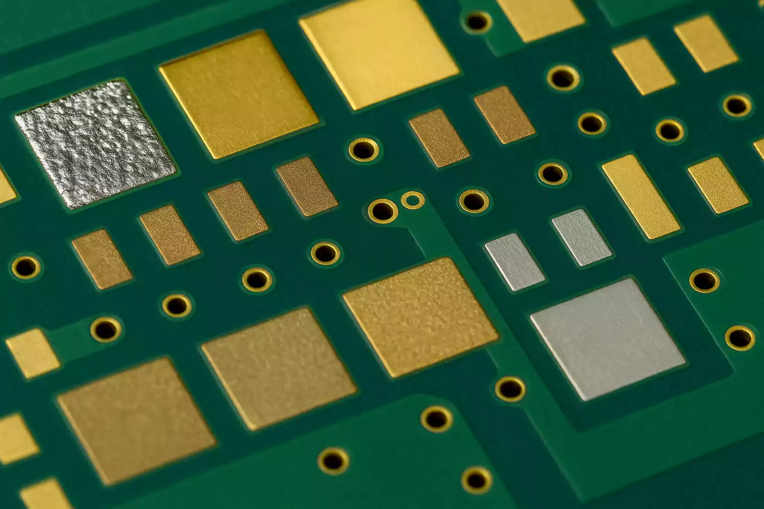
When designing a printed circuit board (PCB), the surface finish you choose affects more than just appearance—it also influences solderability, reliability, shelf life, and cost.
Among all available finishes, ENIG (Electroless Nickel Immersion Gold) stands out as one of the most precise and reliable. It provides excellent planarity, corrosion resistance, and long-term solderability for today’s fine-pitch and high-density designs.
This guide explains what ENIG is, how the process works, standard thickness ranges, the pros and cons, and how ENIG compares with HASL and other finishes. By the end, you’ll know when to choose ENIG and how to avoid common issues such as “black pad.”
What Is ENIG in PCB?
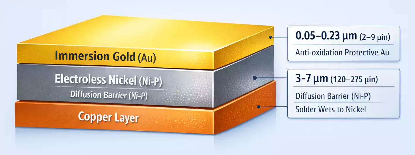
ENIG, short for Electroless Nickel Immersion Gold, is a two-layer metallic coating applied over exposed copper on a PCB.
It combines an autocatalytic nickel layer followed by a thin immersion gold layer. Each plays a critical role in protecting copper and ensuring good solder joints.
The Two-Layer Structure
- Nickel layer (Ni-P):
Acts as a diffusion barrier between copper and solder. It provides the actual solderable surface and prevents copper from migrating into the solder joint. - Gold layer (Au):
Protects the nickel from oxidation and contamination during storage. The gold is skinny—just enough to preserve solderability and low contact resistance.
Once soldering begins, the gold dissolves and the solder bonds directly to the nickel layer.
Typical stackup:
Copper → Nickel (3–7 μm) → Gold (0.05–0.23 μm)
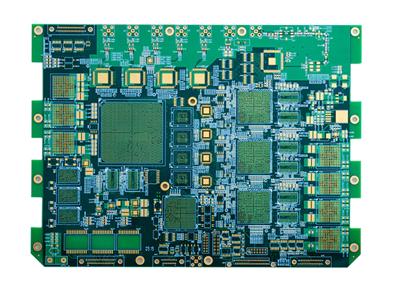
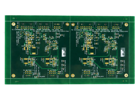
This structure makes ENIG ideal for applications where flatness, corrosion resistance, and long shelf life are critical—such as fine-pitch BGAs, HDI boards, and high-reliability electronics.
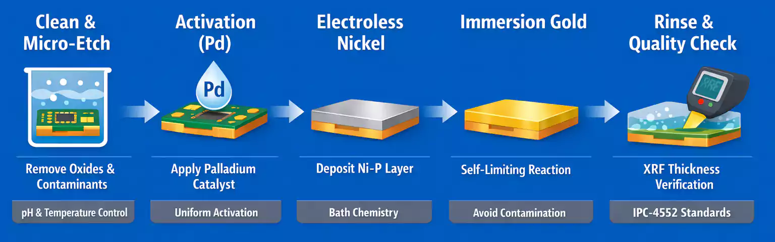
ENIG Plating Process: Step-by-Step
The ENIG process is chemical rather than electrolytic. It relies on autocatalytic reactions rather than an external current. The steps include:
1. Cleaning and Micro-etching
Any contamination, oxidation, or residual flux on the copper surface must be removed. The micro-etch step slightly roughens the surface, improving adhesion of the nickel layer.
2. Activation
A palladium (Pd) catalyst is applied to “activate” the copper surface. This step ensures that the subsequent nickel deposition occurs uniformly across all pads and vias.
3. Electroless Nickel Deposition
Nickel ions in the bath are reduced by a chemical reducing agent (usually sodium hypophosphite) onto the activated surface.
This reaction produces a nickel-phosphorus (Ni-P) layer that’s uniform and self-limiting—no external current required.
Why phosphorus content matters:
Higher phosphorus levels (8–10%) increase corrosion resistance but may slightly reduce solderability. Maintaining proper bath chemistry is key to consistent results.
4. Immersion Gold (Displacement Reaction)
Next, the board is submerged in a gold solution where a chemical displacement reaction occurs: gold ions replace nickel atoms on the surface.
As soon as a thin gold layer covers the nickel, the reaction naturally stops—this is why ENIG gold thickness remains within a narrow, predictable range.
5. Rinsing, Drying, and Quality Inspection
After plating, the board is thoroughly rinsed and dried.
Thickness and uniformity are verified using X-ray fluorescence (XRF) per IPC-4552 standards.
ENIG Thickness and Standards
The IPC-4552 specification defines the recommended thickness for ENIG coatings:
| Nickel (Ni-P) | 3–7 μm | 120–275 μin |
| Gold (Au) | 0.05–0.23 μm | 2–9 μin |
A thicker gold layer doesn’t mean better reliability. Excess gold can increase cost and cause brittle joints (“gold embrittlement”).
Instead, focus on process consistency and thickness uniformity across the board.
Best practice: Always specify ENIG finish as
“ENIG per IPC-4552, Ni: 3–7 μm, Au: 0.05–0.23 μm, measured by XRF.”
Advantages of ENIG Finish
1. Excellent Planarity
Unlike HASL (Hot Air Solder Leveling), ENIG produces a perfectly flat surface, ideal for fine-pitch components, BGAs, and QFNs.
This ensures consistent solder paste printing and joint formation.
2. Superior Corrosion Resistance and Shelf Life
The gold layer prevents oxidation and tarnish, extending storage life well beyond one year in controlled environments.
3. Strong Solderability
Because ENIG maintains a clean, oxide-free surface, solder wetting is reliable even after long storage periods.
It’s also compatible with both lead-free and tin-lead solder processes.
4. Compatibility with Wire Bonding and Test Pads
The nickel-gold surface offers low and stable contact resistance, making it suitable for test points, keypads, and some gold-wire bonding (though ENEPIG is better for that).
Disadvantages and Common Challenges
1. Higher Cost
ENIG involves multiple chemical baths, tight process control, and gold, an expensive material.
Expect ENIG boards to cost 15–25% more than equivalent HASL boards.
2. Risk of “Black Pad.”
Black pad is the most notorious ENIG defect. It’s a corrosion issue at the nickel–phosphorus interface, where overaggressive gold deposition or poor bath control can lead to localized nickel oxidation.
Visually, it appears as dark, non-wettable patches that cause solder joint failure.
Prevention checklist:
- Maintain the pH, temperature, and hypophosphite levels in the nickel bath.
- Regularly filter and refresh the gold bath to avoid contamination.
- Ensure proper rinsing between steps to prevent cross-contamination.
- Verify nickel phosphorus content (typically 7–9%) to improve corrosion resistance.
- Perform XRF and solderability testing for every production lot.
When properly controlled, black pad risk is minimal—but prevention must be built into the process, not inspection.
ENIG vs HASL: Which Is Better?
| Surface Flatness | Excellent | Uneven, especially on fine pitch |
| Solderability | Consistent, oxide-free | Good but may degrade over time |
| Shelf Life | Long (12+ months) | Shorter |
| Cost | Higher | Lower |
| Suitability for BGA/HDI | Excellent | Poor |
| Common Risks | Black pad | Solder bridging, uneven coating |
Conclusion:
Use ENIG for fine-pitch SMT, BGA, and high-reliability applications.
Choose HASL for low-cost, through-hole, or prototype boards where planarity isn’t critical.
ENIG vs OSP, Immersion Silver, and Other Finishes
While ENIG is highly versatile, it’s not always the perfect choice. Here’s how it compares to other popular finishes.
ENIG vs OSP (Organic Solderability Preservative)
- OSP forms a thin organic layer to protect copper.
- It’s inexpensive and very flat but sensitive to handling and storage.
- OSP is suitable for short-term production or single reflow applications, not for harsh or multi-reflow environments.
ENIG vs Immersion Silver
- Immersion silver (ImAg) also provides a flat, solderable surface at a lower cost.
- However, it tarnishes easily, especially in high-humidity or sulfur-rich environments.
- ENIG offers better long-term reliability.
ENIG vs ENEPIG
- ENEPIG (Electroless Nickel Electroless Palladium Immersion Gold) adds a thin palladium layer between the Ni and Au layers.
- It prevents nickel corrosion and supports wire bonding, but costs more.
- Ideal for advanced packaging or high-reliability aerospace/medical boards.
ENIG vs Hard Gold (Electroplated Gold)
- Hard gold is an electrolytic process producing a thicker, wear-resistant layer.
- Best for edge connectors or high-cycle contacts, not soldering surfaces.
- ENIG remains superior for reflow and solder joint reliability.
Selective ENIG: Balancing Performance and Cost
For mixed-technology boards, you don’t always need ENIG everywhere.
Selective ENIG applies a nickel-gold coating only on critical pads, while other regions use OSP or HASL.
Benefits:
- Lower overall cost
- High reliability on key solder or contact areas
- Requires masking and precise process control to separate zones
Use selective ENIG when your board includes both fine-pitch BGA zones and large through-hole areas.
When Should You Use ENIG?
You should specify ENIG when your design meets one or more of the following conditions:
- Fine-pitch SMT or BGA components (<0.5 mm pitch)
- Multi-reflow lead-free assembly
- Long storage or shipping before assembly
- High reliability requirements (aerospace, industrial, medical)
- Flat surface needed for printing or solder paste inspection
- Mixed assembly where consistent wetting is essential
If cost or turnaround is the primary concern, consider OSP or HASL instead.
Troubleshooting and Quality Control
Even with proper process design, ENIG can fail if not monitored.
Here are practical QC measures manufacturers and buyers can apply:
- Incoming Material Check:
Verify surface color (uniform matte gold), no dark spots or discoloration. - Thickness Verification (XRF):
Randomly sample each batch; record Ni/Au thickness within IPC-4552 range. - Solderability Test:
Perform a wetting balance or dip-and-look test after aging. - Storage Conditions:
Store ENIG boards in dry-pack bags with humidity < 40% and temperature < 25 °C.
FAQ
Is ENIG the same as gold plating?
No. ENIG uses a chemical displacement process to deposit a skinny layer of gold, whereas gold plating (electroplated gold) uses an electric current to build a thick, wear-resistant layer. ENIG is for soldering; hard gold is for contact surfaces.
How long can ENIG boards be stored?
When kept sealed and dry, ENIG PCBs can last over 12 months without any degradation in solderability.
What causes black pad?
Black pad results from nickel corrosion during the immersion gold step—usually due to poor bath control, contamination, or over-plating.
Does ENIG work with lead-free solder?
Yes. ENIG is fully compatible with lead-free processes and can handle multiple reflow cycles.
What’s the main reason to choose ENIG over HASL?
For fine-pitch or high-density designs, ENIG’s flat surface ensures consistent solder joints. HASL is cheaper but unsuitable for small-pitch BGAs.
Key Takeaways
- ENIG = Electroless Nickel + Immersion Gold
Two metal layers protect copper and ensure reliable soldering. - Process control matters.
Proper bath chemistry and cleaning prevent black pad and thickness variation. - Use ENIG when precision, reliability, and flatness matter more than cost.
- Specify standards clearly.
Always reference IPC-4552 and thickness ranges in your fabrication notes.
Final Thoughts
In modern PCB manufacturing, ENIG remains the go-to finish for fine-pitch, high-density, and high-reliability designs.
It combines the chemical precision of nickel-phosphorus deposition with the protective benefits of a thin gold layer—delivering exceptional planarity, corrosion resistance, and long-term solderability.
While ENIG costs more and requires tight process control, its consistency and performance make it worth every cent for engineers who value reliability and repeatability.
