

In many compact electronics, EMI problems show up late—often after assembly or early testing. At that point, layout changes are costly. Cable routing is fixed. Mechanical space is tight. And redesign delays the whole schedule.
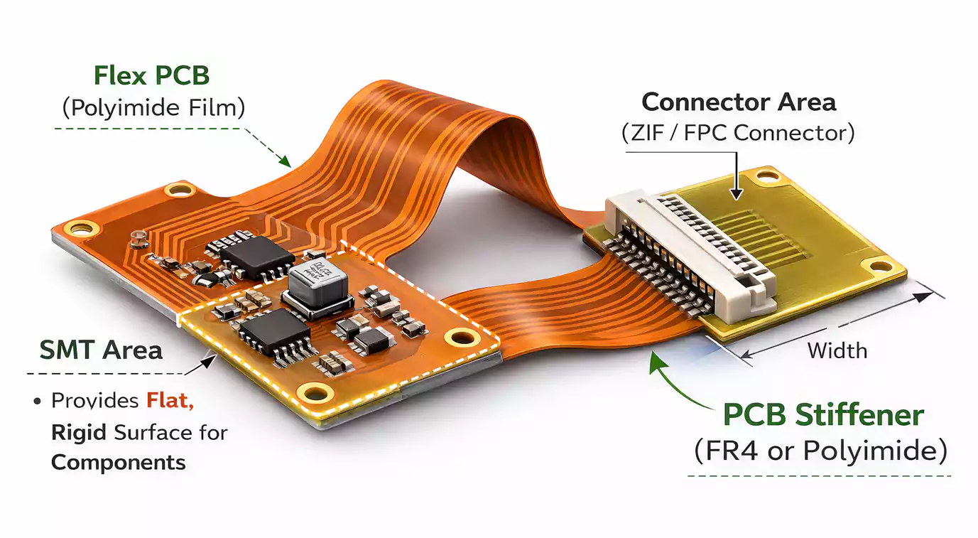
That is why EMI planning matters early, especially for FPC (flexible printed circuits) and rigid-flex PCBs. These designs are used when you need thin routing, tight bending, and high-density packaging. But those same advantages also make EMI harder to control.
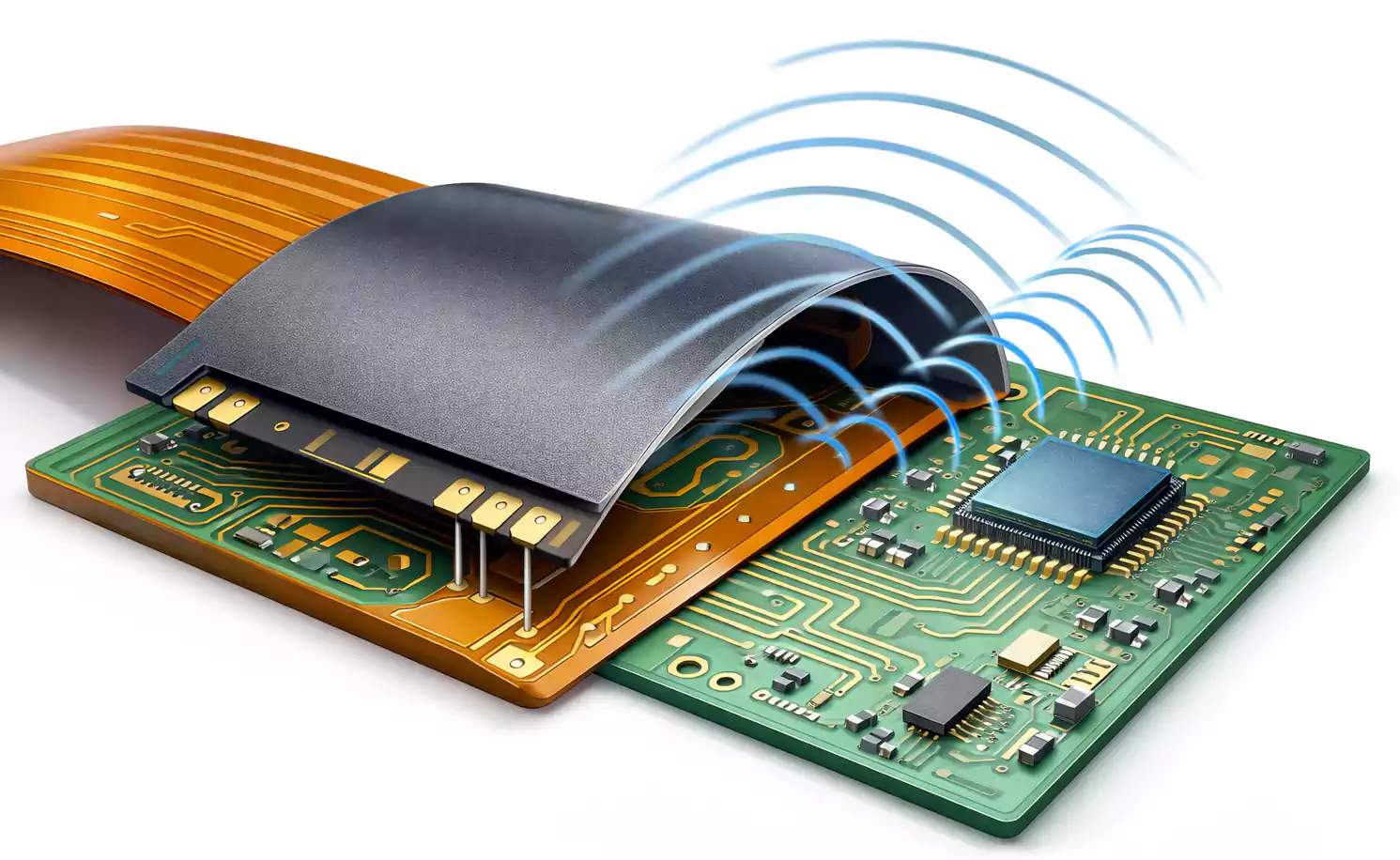
One practical solution is EMI shielding film. It helps reduce interference without adding much thickness or killing flexibility.
Key Takeaways
- EMI shielding film is a thin conductive layer bonded to FPC or rigid-flex PCB surfaces to reduce electromagnetic noise.
- It works best only when it has a reliable ground connection.
- Compared with copper shielding, silver ink, and metal cans, shielding film often offers a better balance of flexibility, thickness, and cost for flex designs.
- Material choice and bonding quality strongly affect real-world performance.
What Is EMI Shielding Film?
EMI (electromagnetic interference) is unwanted electromagnetic energy that can disrupt circuits. It may:
- distort signals
- cause data errors
- reduce performance
- create unstable system behavior
EMI shielding film is a thin conductive material used to block or reduce this interference.
In PCB manufacturing, EMI shielding film is typically bonded onto the surface of:
- FPC (flexible printed circuits)
- Rigid-flex PCBs
You often see it as a dark or black layer on a flexible circuit. But it is not just a protective cover. It is a functional shielding layer designed to control electromagnetic noise.
EMI shielding film must be electrically connected to ground to work effectively.
Why Is EMI Shielding Needed in FPC and Rigid-Flex PCB?
Flexible circuits are used in compact, high-density products. Many of these products include:
- wireless modules (Wi-Fi, Bluetooth, cellular)
- RF antennas
- high-speed processors and memory
- display drivers and camera modules
- sensors, audio, and power converters
When many signal sources are packed into a small space, EMI becomes more likely.
1. Two common EMI risks
- External interference
Noise from nearby devices, power supplies, or wireless signals can enter sensitive circuits. - Internal radiation and coupling
Fast digital edges and RF blocks can radiate or couple into nearby traces, cables, or modules.
2. Why flex makes EMI control harder
FPC and rigid-flex designs must bend and fit into tight spaces. Traditional shielding methods can:
- increase thickness
- reduce flexibility
- Add stress in the bend areas.
- complicate assembly
EMI shielding film helps by improving EMI control while keeping the flex structure thin and workable.
How EMI Shielding Film Works
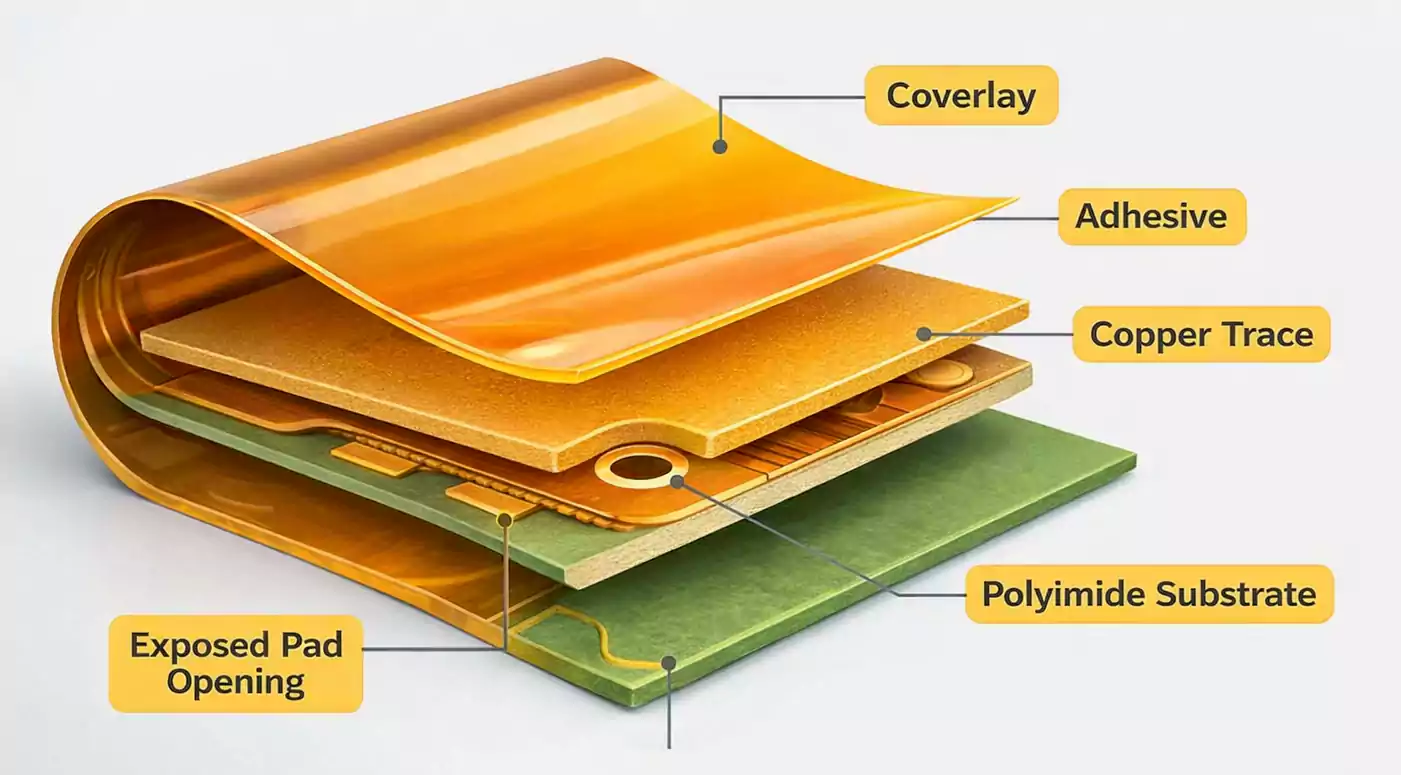
Most EMI shielding films are laminated structures. Exact layer stacks vary, but common elements include:
- Conductive metal layer (the main shielding element)
- Support or insulating layer (often black)
- Conductive adhesive layer (to create electrical contact)
- Optional protective top layers
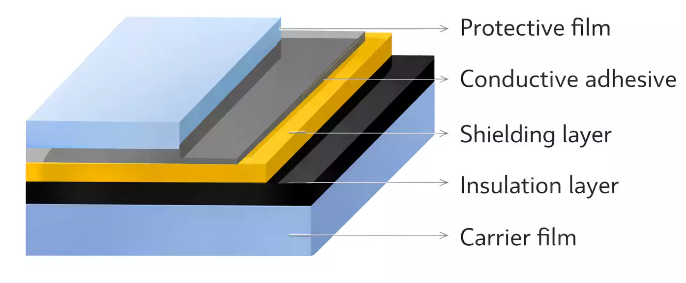
1. The conductive layer
This layer provides the shielding effect. It may be made using:
- metal deposition
- fine copper mesh
- other conductive structures
The conductive layer helps reflect and redirect electromagnetic energy away from sensitive circuits.
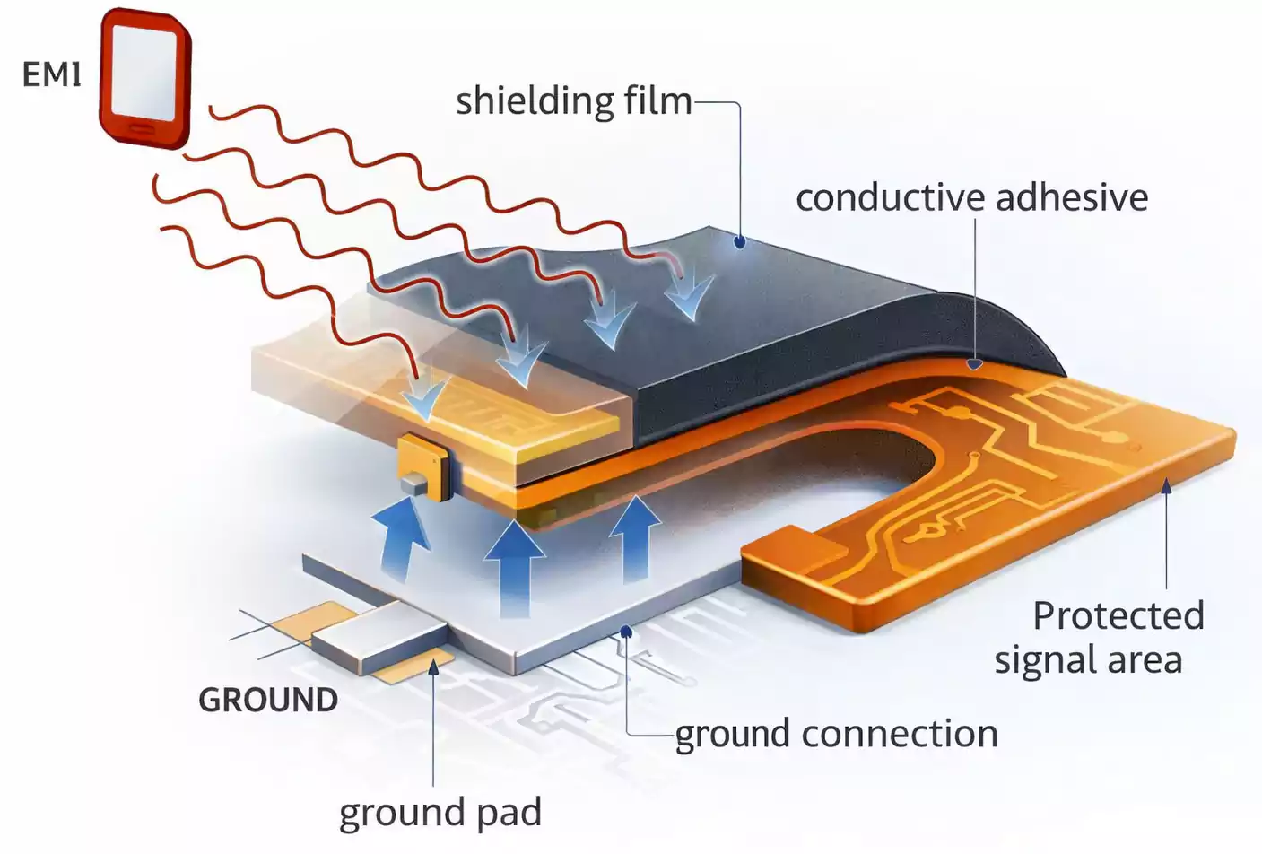
2. Why grounding is critical
Grounding is not optional. It is the difference between “a film on the surface” and “a functioning shield.”
The film typically connects to the ground through:
- designed openings (windows)
- exposed grounding pads
- conductive adhesive contact during lamination
During heat-and-pressure bonding, the conductive adhesive flows and establishes electrical contact between the film and the PCB ground.
Common EMI Shielding Methods for FPC (and How They Compare)
Most FPC EMI strategies fall into these options:
- Copper shielding
- Conductive silver ink
- Metal enclosures (shield cans)
- EMI shielding film
- EMI shielding tape (often used locally)
1. Copper shielding
Pros
- strong EMI performance
- familiar PCB design method
- good electrical control
Cons
- increases thickness and stiffness
- reduces flexibility
- may crack under repeated bending
- Cross-hatched copper improves flex but can reduce shielding.
2. Conductive silver ink
Pros
- thin profile
- moderate flexibility
- can be applied selectively
Cons
- The cost can be high.
- process can be complex (printing + curing + protection)
- performance depends on print quality and coverage
3. Metal enclosures
Pros
- strong localized shielding
- common in rigid PCB assemblies
Cons
- bulky and adds height
- not suitable for flexible areas
- adds assembly complexity
4. EMI shielding film
Pros
- thin construction
- high flexibility
- good fit for compact designs
- strong shielding for many high-speed/RF products
Cons
- requires a good grounding in design
- bonding quality matters a lot
- Placement must respect bend stress zones.
5. EMI shielding tape (where it fits)
EMI shielding tape is often used for local shielding or grounding, such as:
- small areas near connectors
- seams or edges
- quick fixes or assembly-level shielding
- wrapping or local contact points
It is not always a full replacement for a bonded shielding film across a defined flex region.
Quick Comparison Table (FPC EMI Shielding Options)
| Copper Shielding | Low–Medium | High | High | Medium | Controlled designs, rigid areas |
| Cross-hatched Copper | Medium | High | Medium | Medium | Flex with limited bending |
| Silver Ink | Medium | Low | Medium | High | Selective shielding, space tight |
| Metal Enclosure | Very Low | Very High | High (local) | High | Rigid modules, fixed zones |
| EMI Shielding Film | High | Low | Medium–High | Medium | Compact flex, thin devices |
| EMI Shielding Tape | Medium | Low | Medium (local) | Low | Local grounding/shielding |
Key Benefits of EMI Shielding Film
Designers often prefer shielding film in flexible circuits because it delivers a balanced result.
1. Excellent flexibility
It supports bending and folding better than thick metal shielding structures.
2. Minimal thickness increase
This matters for smartphones, wearables, camera modules, and tight connector stacks.
3. Strong high-frequency support
It is well-suited to many modern designs that use RF and high-speed digital signals.
4. Good cost-to-performance balance
In many builds, it is more practical than adding extra copper layers or bulky shielding parts.
EMI Shielding Film vs. ITO and Other Conductive Films
Some EMI shielding films are designed for transparent applications, such as windows or display-related panels. In that space, you may see:
- ITO (Indium Tin Oxide) films
- Copper mesh films
General differences:
- ITO: good transparency, but higher surface resistance
- Copper mesh: lower resistance, stronger conductivity, often better shielding potential
For FPC and rigid-flex PCB, transparency is usually not needed. The priority is:
- conductivity
- flexibility
- grounding reliability
- bonding durability
Typical Applications of EMI Shielding Film
You will commonly see EMI shielding film in products that have:
- high-speed signals
- wireless communication
- dense packaging
- tight mechanical constraints
Common examples
- Consumer electronics: smartphones, tablets, laptops, display modules
- Automotive electronics: control units, communication modules, sensor systems
- Medical devices: monitors and portable diagnostic tools
- Industrial equipment: control systems, communication, and signal processing units
How EMI Shielding Film Is Bonded to an FPC
The bonding process is straightforward, but it must be controlled carefully.
1. Standard bonding steps
- Cut to size based on the design outline.
- Remove the release liner to expose the adhesive layer.
- Align and place the film on the target area.
- Laminate under heat and pressure.
- Form ground contact as a conductive adhesive connects to ground pads/openings
- Inspect adhesion, alignment, and electrical continuity.
2. Common mistakes to avoid
- poor grounding layout (not enough contact points)
- incomplete adhesive contact
- weak lamination pressure or uneven bonding
- placing film across high-stress bend zones without planning
- ignoring the bend radius during material selection
How to Choose the Right EMI Shielding Film
Use these practical checks. They match how engineers actually decide.
1. Flexing requirement
- Is it a static bend (installed once) or a dynamic bend (repeated movement)?
The dynamic bend needs better mechanical tolerance.
2. EMI target and frequency range
- Are you controlling RF noise, high-speed digital edge radiation, or mixed-signal coupling?
Different noise types need different shielding strategies.
3. Thickness limit
- Do you have strict mechanical limits near connectors, displays, or housings?
Film is often chosen because the thickness is limited.
4. Grounding design quality
Ask:
- Where does the film contact ground?
- Are openings and pads designed clearly?
- Is the ground path continuous and reliable?
5. Reliability environment
Consider:
- heat and thermal cycling
- vibration and handling
- humidity and long-term adhesion
- assembly flow and inspection capability
A good choice balances EMI performance with flexibility, thickness, manufacturability, and cost.
FAQ
Is EMI shielding film the same as coverlay?
No. Coverlay protects traces mechanically and electrically. EMI shielding film is conductive and is used to reduce EMI. It must be grounded to work.
Does EMI shielding film always need grounding?
Yes, in most PCB use cases. Without a reliable ground connection, shielding effectiveness drops sharply.
Is EMI shielding film better than copper shielding?
It depends. Copper can provide very strong shielding and may suit some controlled designs. Film is often better when you must keep thickness low and flexibility high.
Can EMI shielding film be used in a rigid-flex PCB?
Yes. It is commonly used to protect signal paths in flex regions while keeping the stack thin.
When should I use EMI shielding tape instead of film?
Tape is often used for local shielding, seams, edges, or assembly-level grounding. Film is more suitable for defined shielding coverage across a flex region.
Conclusion
EMI shielding film is a practical solution for FPC and rigid-flex PCB designs. It helps reduce electromagnetic interference while keeping circuits thin and flexible. That is why it is widely used in compact, high-speed, and wireless electronics.
As electronics continue to evolve, EMI control will remain essential. FastTurnPCB supports engineers and manufacturers with fast, reliable PCB solutions built for today’s high-performance applications.
