As PCB designs become smaller, denser, and more performance-driven, surface-mounted components alone are no longer the most efficient option. That is why embedded resistors are becoming more common in advanced PCB design.
Among embedded components, embedded resistors are among the most mature and widely used. The most established type is the thin-film embedded resistor, also known as a formed embedded resistor or planar resistor, which plays an important role in embedded passive technology.
This article examines how embedded resistors work, how they are formed on the PCB, and the process controls needed to maintain resistance accuracy and support good signal integrity.
Why Use Embedded Resistors
As electronic products become smaller and more function-dense, PCB space becomes harder to manage. In many designs, embedded resistors provide a practical way to improve layout efficiency and electrical performance.
1. Save surface space
Conventional resistors occupy valuable board surface area. Embedding them inside the PCB frees space for other components and gives designers more routing flexibility.
2. Reduce via usage
Embedded resistors can also reduce the need for some vias associated with surface-mounted parts, which is especially helpful in high-density layouts.
3. Support smaller PCB designs
By moving passive components into the board structure, designers can build more compact layouts and, in some cases, reduce the overall PCB size.
4. Improve signal integrity
In high-speed, high-density applications, embedded resistors on PCB are used not only to save space but also to improve signal integrity. This is one reason formed embedded resistors are attractive in advanced board design.
Main Types of Embedded Resistors
Embedded resistors are available in several forms, but the thin-film embedded resistor remains the most widely used and mature option. In advanced PCB design, this is usually what the technology engineers mean when they refer to embedded resistors.
What Is a Thin-Film Embedded Resistor
A thin-film embedded resistor, also called a formed embedded resistor or planar resistor, is made by laminating resistive foil with a dielectric material and then defining the resistor geometry through a subtractive PCB process.
This approach is one of the most established solutions in embedded passive technology.
Thin-film embedded resistors can be formed on either inner layers or outer layers. An inner-layer resistor is especially useful when surface space is limited and routing density is high.
The resistive foil can be laminated with several dielectric materials, including:
- FR-4
- polyimide
- PTFE
As a result, this technology is not limited to standard rigid PCBs. It can also be used in flexible printed circuits, making it suitable for compact and specialized designs.

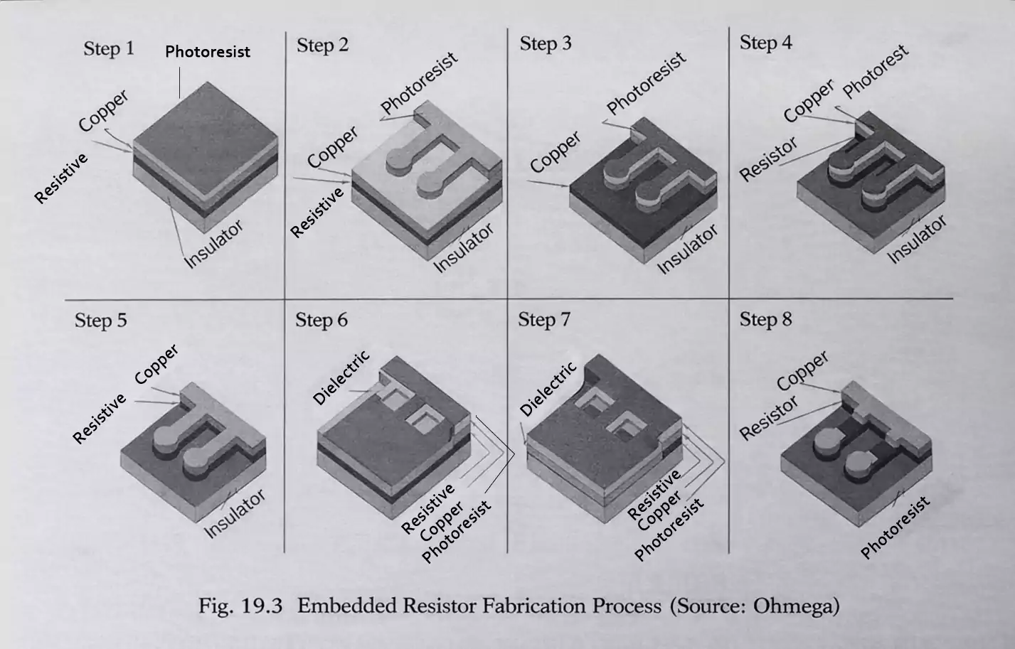
Embedded Resistor Process Flow
The embedded resistor process for thin-film embedded resistors uses photolithography and selective etching. The goal is to define both the copper and resistor patterns with sufficient precision to achieve the required resistance value. In most cases, the resistor etching process includes eight main steps.
Step 1: Apply photoresist
A layer of photoresist is coated onto the material surface to prepare for imaging and pattern transfer.
Step 2: Expose and develop the pattern
The photoresist is exposed and developed to create the required pattern, including both copper and resistor features.
Step 3: Etch away unwanted copper
A conventional etchant removes the excess copper and forms the initial copper pattern.
Step 4: Etch away the unwanted resistive layer
A copper sulfate solution is used to remove the unwanted resistive layer. This step helps maintain copper etching accuracy, allowing the copper pattern to be controlled precisely.
Step 5: Strip the resist
After the first two etching steps, the photoresist is removed.
Step 6: Reapply photoresist and develop again
A new photoresist layer is applied and developed to define the next copper-and-resistor pattern for final shaping.
Step 7: Selectively etch copper to expose the resistor
An alkaline etchant is used to selectively remove copper and expose the resistor area that must remain. This is one of the most critical steps in the process, because the resistor must be exposed accurately without damaging the resistive material.
Step 8: Strip the resist again
The remaining photoresist is removed, completing resistor formation.
Why Embedded Resistors Require Three Etching Steps
A thin-film embedded resistor is not formed in a single etch. The process uses three separate etching steps, each with a specific role.
1. First etch
Removes unwanted copper and forms the initial copper pattern.
2. Second etch
Removes the unwanted resistive layer while maintaining copper pattern accuracy.
3. Third etch
Removes copper selectively to expose the finished resistor without damaging the resistive material.
Although this multi-step embedded resistor process is more complex, it provides much better control over copper and resistor geometries and the final resistance value.
How Outer-Layer Embedded Resistors Are Protected
When an embedded resistor is formed on an outer layer, it can be protected with solder mask ink. This helps reduce surface damage and improves stability during later processing and end use.
Manufacturing Requirements for Embedded Resistors in PCB
Embedded resistors in PCB are a mature technology, but they still require tight process control.
1. Etching must be precise
Final resistance depends not only on the resistive material, but also on the size and shape of the resistor pattern. Any etching error can change the geometry and shift the resistance value.
2. The resistor must be protected after exposure
Once the resistor area is exposed, each subsequent process step must be carefully controlled to prevent chemical attack on the resistor surface. Surface changes can lead to resistance drift.
Which Later Processes Can Affect Resistance Value
Resistance is affected not only by resistor formation, but also by later PCB manufacturing steps. Common examples include:
- pre-solder-mask treatment
- inner-layer browning or oxide treatment
These steps often use acidic micro-etch solutions, which can affect the resistor surface and change the final resistance value.
For that reason, embedded resistors must be evaluated within the context of the full downstream manufacturing flow, not as an isolated feature.
How Resistance Shift Is Controlled in Production
To reduce resistance variation caused by later processing, manufacturers usually combine process control with front-end compensation.
1. Control pre-solder-mask treatment chemistry
The treatment solution and process window can be adjusted to reduce their effect on the resistor surface.
2. Optimize the browning or oxidation process
The browning process should support reliable layer bonding while minimizing damage to the resistive layer.
3. Use CAM for front-end compensation
When later process steps are expected to shift resistance, computer-aided manufacturing (CAM) can be used to compensate in advance. The resistor geometry or target value is adjusted at the front end so the finished board is closer to the required resistance after the full manufacturing process.
This is best understood as a design-and-manufacturing control strategy, not a correction from a single process step.
Key Factors in Resistance Accuracy Control
Resistance accuracy depends on tight control of a few critical process variables.
1. Control the etch endpoint
One of the most important factors is control of the etch endpoint. The etch must stop at the correct point, since over-etching or under-etching will affect the final resistor dimensions.
2. Keep resistor geometry accurate
Resistance accuracy depends directly on how closely the final resistor geometry matches the design.
3. Minimize surface damage
Electrical performance is influenced not only by resistor shape, but also by surface condition. For that reason, the resistive surface must be protected throughout manufacturing.
4. Control processes that can attack the resistor surface
Special attention should be given to processes such as:
- acid cleaning
- micro-etching
- oxidation
If these steps are not tightly controlled, they can alter the resistor surface and reduce resistance stability.
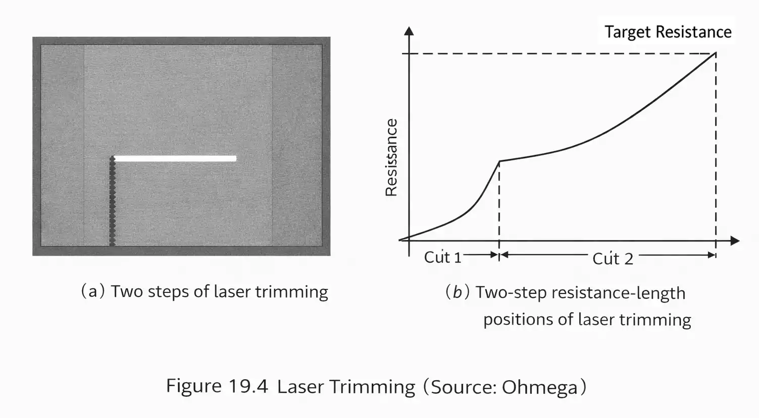
What to Do When Higher Precision Is Required
For tighter resistance tolerances, standard etching control may not be enough. In those cases, laser trimming is often used.
Laser trimming adjusts the resistor after formation, enabling tighter final tolerance. In high-precision applications, it is an important post-process correction method.
In discussions of embedded passive technology, names such as OhmegaPly may also come up in connection with resistive-foil-based structures. In practice, the main engineering priorities remain material compatibility, geometry control, and final resistance stability.
Advantages and Engineering Trade-Offs of Embedded Resistors
From both design and manufacturing perspectives, embedded resistors offer clear benefits, but they also introduce process challenges.
1. Main advantages
- Save PCB surface space
Less surface area is consumed by discrete passive components.
- Reduce via usage
This supports higher routing density in compact designs.
- Enable a smaller PCB size
Embedding passive components can help reduce overall board size and improve packaging efficiency.
- Improve signal integrity
This is one of the key advantages of a formed embedded resistor and similar built-in passive structures.
- Support multiple dielectric systems
The technology can be used with FR-4, polyimide, PTFE, and other materials.
- Work in rigid and flexible circuits
That makes the technology suitable for a wider range of applications.
2. Main challenges
- High etching precision is required
Any error in resistor geometry directly affects the final resistance value.
- Downstream process compatibility matters
Once the resistor is exposed, it must be protected from later chemical attack.
- Resistance can shift during later chemical processing
Acidic micro-etch steps can change resistance, so both process optimization and front-end compensation are needed.
- High-precision designs may require laser trimming
This adds manufacturing complexity and tighter process control requirements.
Because of that, engineers need to balance size, electrical performance, process capability, tolerance, and cost when deciding whether to use embedded resistors in PCB.
Conclusion
Embedded resistors are one of the most established technologies in advanced PCB manufacturing, with thin-film embedded resistors being the most widely used form. They help save surface space, reduce via usage, support smaller board designs, and can improve signal integrity.
From a manufacturing perspective, success depends on controlled use of resistive foil, accurate photolithography and etching, and careful management of downstream processes that can affect resistance value. In tighter-tolerance applications, laser trimming may also be required.
For PCB designers and manufacturers, embedded resistors in PCB are not just a way to save space. They are a practical design approach for improving integration, controlling electrical performance, and making better use of board area.