


If you’ve ever looked at a printed circuit board (PCB) and wondered what all those tiny components do—you’re not alone. Whether you're just getting started in electronics or you're troubleshooting a complex assembly, knowing how to identify components on a PCB is essential.
This guide offers a clear, visual walkthrough of the most common electronic components found on PCBs—complete with real-world examples, identification tips, and practical insights into how these parts work together. You’ll find a structured PCB components list with pictures, an easy-to-understand components diagram, and actionable advice to help you spot parts by their reference designators, orientation markings, and physical features.
Electronic Components PCB at a Glance
Before diving into the full component list, let’s first get familiar with a few important concepts that will make things much easier:
Active vs. Passive Components
- Active components include integrated circuits (ICs), transistors, and voltage regulators. These devices need power to function and can control or amplify electrical signals.
- Passive components, like resistors, capacitors, and inductors, don’t require power to operate. Instead, they store, filter, or control electrical energy passively within a circuit.
Through-Hole vs. Surface Mount (SMD)
- Through-hole components have long metal leads that are inserted into holes drilled in the PCB and soldered from the opposite side.
- Surface mount components are much smaller and sit directly on the surface of the board. They’re the standard in today’s high-volume, automated manufacturing because they save space and assembly time.
Most modern PCBs use a mix of both—SMD parts for efficiency, and through-hole parts where mechanical strength or high power handling is required (like connectors or large capacitors).
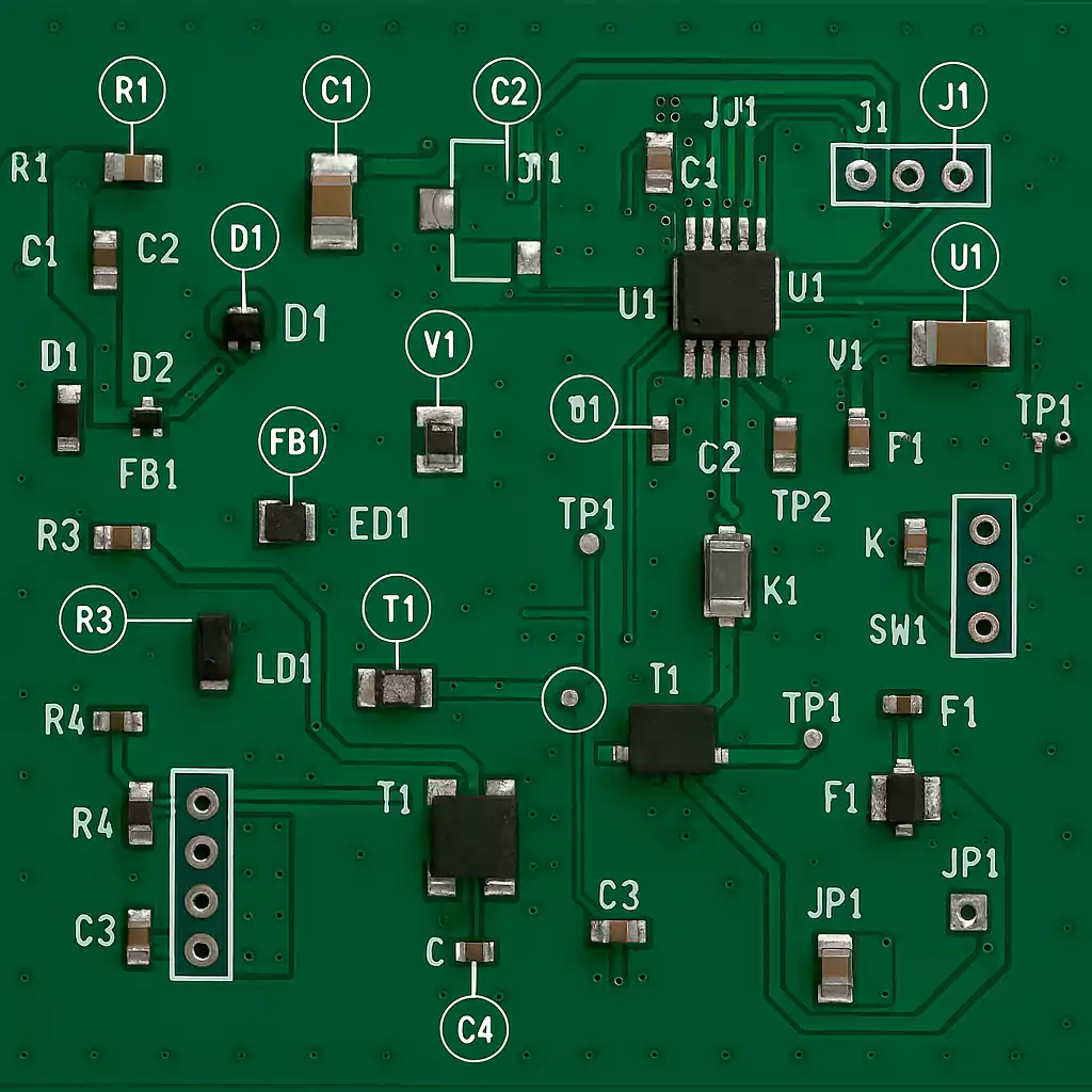
Common Designators
| Symbol | Component | Notes |
|---|---|---|
| R | Resistor | Limits or divides current |
| C | Capacitor | Stores energy, filters noise |
| L | Inductor | Filters, stores magnetic energy |
| D | Diode | One-way current flow |
| LED | Light-Emitting Diode | Visual indicators |
| Q | Transistor/FET | Switching and amplification |
| U/IC | Integrated Circuit | Logic, control, processing |
| Y/XTAL | Crystal/Oscillator | Timing and frequency control |
| J/P | Connector or Header | Input/output connections |
| SW | Switch | User input, toggles |
| F | Fuse | Overcurrent protection |
| FB | Ferrite Bead | Suppresses high-frequency noise |
| TP | Test Point | Debug and measurement access |
| T | Transformer | Isolation or voltage change |
| K | Relay | Electromechanical switch |
| JP | Jumper | Configurable connection |
The Complete Electronic Components PCB List (with Pictures)
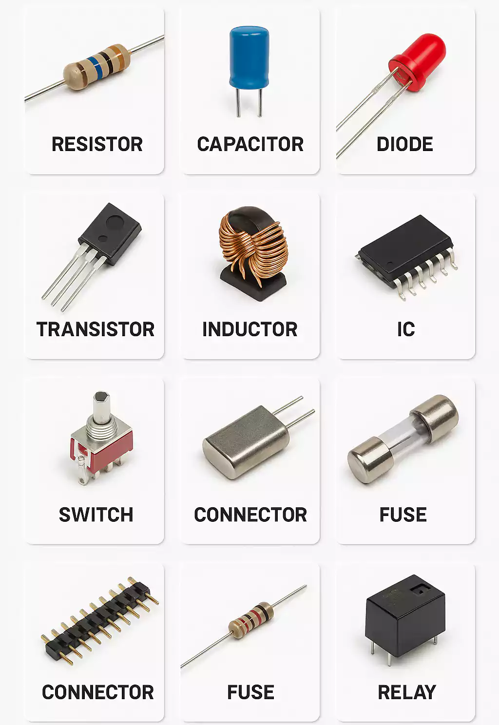
- Resistors (R)
Purpose: Limit current, set bias points, form dividers, pull-ups/downs.
Common packages: 0603/0805 SMD; axial for through-hole.
Identification: Rectangular SMD bricks; through-hole have color bands (value code).
Gotchas: Misreading “0Ω jumpers” as true resistors. - Capacitors (C)
Purpose: Bypass, decouple, filter, and timing.
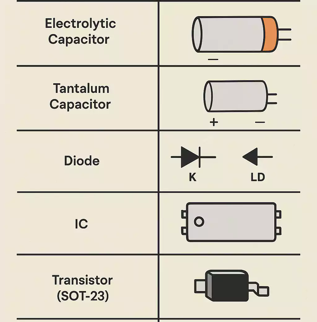
Types: Ceramic (non-polar), Electrolytic (polar), Tantalum (polar), Film (non-polar).
Identification: Ceramics are small beige SMD blocks; electrolytics are cans with a negative stripe; tantalums often have a positive (+) mark.
Gotchas: Reversing electrolytic/tantalum polarity; picking too low a voltage rating. - Inductors / Chokes (L)
Purpose: Store energy in magnetic fields, filter (LC), buck/boost supplies.
Identification: SMD cubes or donuts; through-hole toroids or wire-wound cylinders.
Gotchas: Confusing inductors with resistors or ferrite beads; watch current rating and DCR. - Diodes (D)
Purpose: Rectification, clamping, steering, protection (TVS).
Polarity: Stripe = cathode (K).
Variants: Schottky, Zener, TVS.
Gotchas: Installing backward kills protection; choosing the wrong reverse standoff for TVS. - LEDs (LED / D)
Purpose: Indicators, optical outputs.
Polarity: Flat edge or shorter lead = cathode (K); SMD often shows a triangle or notch.
Gotchas: Current limiting is mandatory—never run LEDs without a resistor or proper driver. - Transistors & MOSFETs (Q)
Purpose: Switching, amplification, level shifting, load control.
Packages: SOT-23, SOT-223, TO-220, DFN/QFN.
Identification: Look for a Pin-1 dot or bevel; datasheet orientation matters.
Gotchas: Swapping source/drain on FETs; under-sizing Rds(on) or gate drive. - Integrated Circuits (U / IC)
Purpose: Everything from op-amps to microcontrollers, PMICs, codecs, and RF SOCs.
Pin 1: Always locate the dot, notch, or chamfer; on BGAs, a silkscreen triangle.
Common packages: SOIC/TSSOP (leaded), QFN/QFP (leadless/leaded), BGA (array).
Gotchas: Rotating 90° off; insufficient thermal pad solder on QFN; handling ESD-sensitive parts. - Crystals & Oscillators (Y / XTAL)
Purpose: Timing reference for MCUs, radios, and clocks.
Identification: Metal cans or tiny ceramic packages; marked frequency (e.g., 8.000 MHz).
Gotchas: Wrong load capacitance on crystals; mixing XO/TCXO/OCXO requirements. - Connectors & Headers (J / P)
Purpose: Power, I/O, programming, external modules.
Types: Pin headers, board-to-board mezzanines, USB, barrel jacks, FFC/FPC, terminal blocks.
Gotchas: Orientation and keying; current rating on power connectors; E-mark needs for USB-C. - Switches & Buttons (SW)
Purpose: User input, reset, power toggles.
Types: Tactile, slide, DIP, rotary encoders.
Gotchas: Debounce needs; through-hole vs. SMD mechanical robustness. - Fuses (F)
Purpose: Over-current protection.
Identification: SMD “F” markings or glass cartridge for through-hole.
Gotchas: Slow-blow vs. fast-acting selection; voltage drop and hold current. - Ferrite Beads (FB)
Purpose: High-frequency noise suppression on power and signal lines.
Identification: Looks like a small inductor; labeled FB in BOM/silkscreen.
Gotchas: Choose based on impedance vs. frequency and current rating, not DC value. - Transformers (T)
Purpose: Isolation, voltage step-up/down, PoE, SMPS.
Identification: Larger magnetics, often with bobbins or shielding.
Gotchas: Watch isolation voltage, leakage inductance, and core losses. - Relays (K)
Purpose: Galvanic isolation for switching higher voltages/currents.
Identification: Boxy packages with pin diagrams on top.
Gotchas: Flyback diodes on coils; contact ratings vs. actual load type (inductive vs. resistive). - Sensors (varies; often U/IC)
Purpose: Temperature, IMU, light, pressure, humidity, Hall-effect.
Gotchas: Orientation (e.g., IMU axes), placement (light/air paths), and pull-up requirements. - Heatsinks & Mechanical Hardware
Purpose: Thermal management and structural support.
Gotchas: Clearance to keep-out zones; thermal pad paste vs. tape; airflow direction. - Test Points (TP)
Purpose: Probing, ICT, programming.
Identification: Labeled pads or vias; sometimes colored rings.
Gotchas: Spacing and accessibility; ensure solid ground reference points. - Jumpers / Links (JP)
Purpose: Reconfigurable options (voltage select, boot mode).
Gotchas: Clear silkscreen for default position; document consequences of each setting. - Antennas & RF Components
Purpose: Wireless connectivity (BLE, Wi-Fi, LoRa, GNSS).
Gotchas: Keepout under antennas, controlled impedance lines, matching networks near the feed. - Potentiometers / Trimmers
Purpose: Adjustable voltage/current setpoints, calibration.
Gotchas: Access for screwdriver; ensure rotation orientation matches silkscreen. - Displays
Purpose: 7-segment, character LCDs, TFTs, e-paper.
Gotchas: Backlight power, contrast bias rails, connector fragility. - Modules (Power/Radio/Compute)
Purpose: Drop-in functionality (DC-DC, ESP32, LTE modems, GNSS).
Gotchas: Shield clearance, regulatory labeling, and keepouts for RF.
How to Identify Components on a Circuit Board
Learning to recognize components on a PCB comes down to three main skills: reading the silkscreen, checking polarity, and recognizing common packages. Here’s how to do it efficiently.
1. Use the Silkscreen and Reference Designators
Most PCBs have a silkscreen layer—white markings printed next to each component. These include reference designators like:
- R = resistor
- C = capacitor
- U = integrated circuit
- D = diode
- Q = transistor
- J/P = connector
2. Check Polarity and Orientation
Some components only work in one direction. Common polarity cues include:
- Electrolytic capacitors: A stripe marks the negative side.
- Tantalum capacitors: A “+” sign shows the positive side.
- Diodes & LEDs: The stripe or flat edge marks the cathode (–).
- ICs: Look for a dot or notch indicating Pin 1.
- Transistors: Don't assume pin order—check the part number and datasheet.
3. Recognize Common Packages and Sizes
- SMD passives: 0603, 0805, 1206—bigger numbers mean bigger size.
- Leaded ICs: SOIC, TSSOP—look for a notch to find Pin 1.
- Leadless ICs: QFN/DFN packages often have a large thermal pad underneath.
- Power components: TO-220 and SOT-223 are usually mounted near heatsinks.
4. Use Circuit Context (If No Schematic)
Even without documentation, you can often guess a component’s role based on its location:
- Capacitors near ICs = decoupling.
- Resistors near signal lines = pull-ups or pull-downs.
- Inductors + capacitors at power input = filtering or regulation.
Selection & Substitution Guide
When a component is out of stock or you need a better-suited alternative, choosing the right substitute is about functionality, safety, and fit. Here's how to do it right:
1. Match the Function
Don’t assume any similar-looking part will do. For example:
- A TVS diode for ESD protection is not the same as a power rectifier.
- A ferrite bead is not an inductor—they suppress high-frequency noise, not store energy.
2. Respect the Essentials
- Polarity & Pinout: These must match exactly. Reversing polarized parts (like diodes, LEDs, or electrolytics) can damage the board.
- Electrical Ratings:
- Capacitors: Use voltage ratings ≥1.5× your circuit's working voltage.
- MOSFETs & Transistors: Check Vds, Id, and Rds(on).
- ICs & regulators: Mind the current handling, dropout voltage, and quiescent current.
- Frequency Behavior:
- Crystals must match the required load capacitance.
- Op-amps need suitable gain-bandwidth product (GBW) and slew rate.
- Ferrite beads and inductors behave differently across frequencies—check datasheets.
3. Fit Matters
- Package & Footprint: Substitutes must fit both electrically and mechanically. Even common SMD packages like 0603 and 0805 vary slightly in pad dimensions. For ICs, QFN/QFP body size and pad pitch are critical.
4. Performance Tolerances
- Resistors: Tolerance (±1% is common), temperature coefficient, and power rating.
- Capacitors: Dielectric type (X7R, NP0), ESR, and ripple current capability.
5. Plan for Heat & Aging
- Use voltage derating for caps and heatsinking for power devices.
- Choose components with stable temperature ratings and avoid known EOL (end-of-life) parts.
Common Mistakes & Troubleshooting
Even experienced engineers make mistakes during assembly or rework. Here are common pitfalls—and how to avoid them:
1. Reversed Polarity
Most frequent with:
- Electrolytic or tantalum capacitors (look for stripe or “+” sign)
- Diodes and LEDs (stripe = cathode)
Symptoms: Component heating, no LED illumination, or full failure.
2. IC Orientation Errors
A rotated IC—especially in SOIC or QFN packages—can short power lines. Always double-check Pin 1 (dot, notch, or bevel) against the silkscreen before soldering.
3. Package Confusion
- SOT-23 vs. SOT-89 vs. SOT-223: Visually similar but electrically and mechanically different.
- Ferrite bead vs. resistor: Both may be small black SMDs—check the designator: FB vs. R.
- PTC resettable fuse vs. resistor: Same shape, different function—marked F.
4. Soldering Issues
- Bridging: Common with fine-pitch ICs (QFP, QFN).
- Cold joints: Result from insufficient heat or paste, especially under thermal pads.
- Lifted pads: Caused by overheating during rework or excessive solder wick use.
5. Quick Checks Before Power-Up
- Use diode mode on a multimeter to test diodes, LEDs, and transistor junctions.
- Check for continuity across power rails—no shorts to ground.
- Use a microscope or magnifier to confirm polarity markings, silkscreen labels, and solder joint quality.
Conclusion
This guide has covered the essentials of identifying electronic components on a PCB—from reading silkscreen markings and reference designators to spotting polarity indicators and recognizing common packages.
By focusing on key visual cues like stripes, dots, and notches, and understanding how electronic components PCB are labeled and placed, you can confidently identify parts and avoid costly mistakes during assembly, repair, or troubleshooting.
