


If you love guitar pedals, you’ve probably thought about building one yourself.
Every effect pedal—from fuzz and overdrive to chorus and delay—has a small printed circuit board (PCB) inside. That board is the heart of the effect. It connects components, routes audio signals, and controls how power and tone flow through your circuit.
This guide explains what an effect pedal PCB is, how it’s designed, and how to turn your DIY idea into a reliable, professional-quality build. Whether you’re wiring your first stompbox or planning a small-batch production, this article will help you design, test, and manufacture a clean, low-noise board.

What Is an Effect Pedal PCB?
An effect pedal PCB is a small printed circuit board that holds and connects all the electronic parts of a guitar or instrument pedal. Instead of using messy wires or breadboards, a PCB uses copper traces to connect resistors, capacitors, chips, switches, and jacks.
There are three main ways hobbyists build pedals:
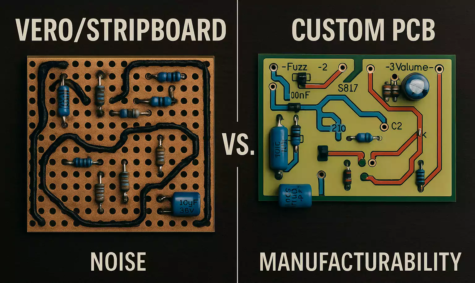
- Stripboard or perfboard (vero board): Great for learning and prototyping, but easy to make wiring mistakes and hard to repeat.
- Hand-wired or point-to-point: Classic for vintage effects, but not ideal for consistency or mass production.
- Custom PCBs: The professional method—cleaner signal paths, stronger mechanical support, and far more repeatable results.
That’s why most DIY pedal builders eventually switch to PCB layouts. You can design your own from a schematic or download one from a community site like Effects Layouts. The result is a cleaner, quieter, and more durable build.
From Circuit to PCB: A Step-by-Step Design Process
Designing a pedal PCB is both fun and rewarding. Below is a simple process used by professionals and hobbyists alike.
Define your goal
Start by listing what you want the pedal to do.
Is it a distortion, compressor, or delay?
What voltage will it use (9 V, 12 V, or 18 V)?
How big is the enclosure?
Defining the mechanical and electrical limits helps you plan the layout before drawing anything.
Draw the schematic
Every good PCB starts with a verified schematic. You can recreate a known circuit, combine modules (like buffer + tone stack), or design your own.
When drawing, label every resistor, capacitor, diode, and IC clearly. Check pinouts twice—especially for transistors and op-amps.
Choose your components
Select reliable components that fit the enclosure. Potentiometers, 3PDT footswitches, jacks, and LEDs all have different footprints.
Common pedal parts include:
- TL072, NE5532, or LM741 op-amps
- 1N4148 or germanium diodes for clipping
- Metal film resistors for low noise
- Aluminum electrolytic and film capacitors
Keep lead spacing standard so your parts fit easily when ordering PCBs or assembly services.
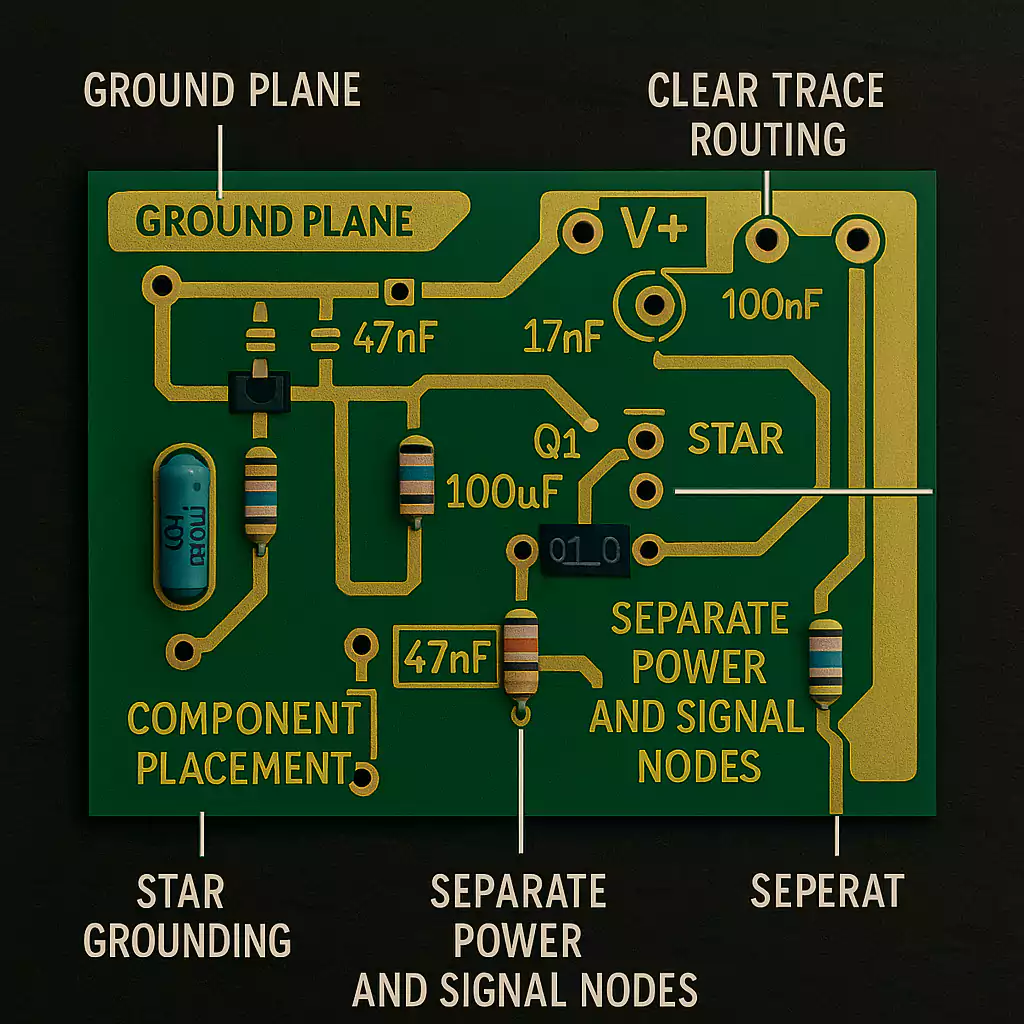
Layout like a pro
Layout is where electrical design meets physical reality. Follow these golden rules:
- Signal flow: Route from input to output in one direction. Avoid looping traces.
- Grounding: Use a single-point (star) ground or separate analog and power grounds. Keep input ground isolated from noisy sections.
- Power routing: Add decoupling capacitors (0.1 µF near each IC, plus larger 10–47 µF caps).
- Protection: Add reverse-polarity protection diodes and a small series resistor at the power input.
- Noise control: Keep high-gain stages short and shielded. Avoid running signal lines next to the DC jack or LED wiring.
- Mechanical design: Align pots, switches, and jacks with your enclosure. Use board-mounted hardware to reduce hand-wiring and improve reliability.
Double-check your layout by printing it at 1:1 scale and comparing it to the enclosure before ordering boards.
Check manufacturability (DFM)
Before fabrication, verify that:
- Minimum trace/space meets fab rules (typically 6 mil/6 mil).
- Vias have enough annular ring.
- Text and polarity marks are readable.
- Silkscreen doesn’t overlap pads.
- You’ve exported the correct Gerber, drill, and BOM files.
Professional PCB manufacturers can often review your Gerbers and point out errors before production.
Prototyping and testing
When your first boards arrive, solder one carefully.
Check for shorts, then power up with a current-limited supply. Test each stage with an audio probe or oscilloscope.
Document any corrections so you can finalize the layout for small-batch builds.
DIY vs. Professional Manufacturing
DIY methods like toner transfer or etching are fun and educational. They’re fine for single-sided boards or quick experiments. However, they can have uneven traces, poor solder mask, and limited repeatability.
Professional PCB fabrication—such as a quick-turn service—offers:
- Multilayer or double-sided boards
- Clean solder mask and plated vias
- Consistent copper thickness
- Optional assembly (PCBA) services
When you’re building more than one pedal or planning to sell your designs, moving to professional production ensures consistent tone, lower noise, and a professional appearance.
Typical Circuits and Layout Tips
Different pedal types have different layout needs.
Fuzz, Overdrive, Distortion
These high-gain circuits amplify everything—including noise.
Keep input traces short and far from power lines.
Use star grounding and separate high-current LED lines from the audio path.
Mount pots and jacks directly on the board to avoid long, noisy wires.
Delay, Chorus, or Modulation
Time-based effects use clock or digital chips. Keep the clock section isolated from the analog audio path.
Add ground shields around oscillators and analog-to-digital converters.
Use separate ground returns for audio and digital sections.
Buffer or Booster
These are simple but sensitive.
Place the input capacitor and resistor close to the jack.
Avoid ground loops by tying all grounds at one point near the power input.
Assembly and Testing: From “It Works” to “It’s Reliable”
Even a great PCB can fail if assembled poorly. Follow these best practices:
- Clean soldering: Use fresh solder and flux. Dull or cracked joints cause intermittent noise.
- Component placement: Match polarity marks (electrolytic caps, diodes, LEDs).
- Mechanical fit: Check that pots and jacks align with the enclosure before soldering.
- Cleaning: Remove excess flux or fingerprints with isopropyl alcohol to avoid leakage paths.
- Testing: Add test points for signal and power rails. Verify voltage before final assembly.
Professional builders often perform a quick burn-in test—running the pedal for several hours to ensure stability.
Cost and Lead Time: From Prototype to Small Batch
Small PCB runs are now affordable and fast.
Typical lead times are:
- Prototype (1–5 pcs): 3–5 days
- Small batch (20–100 pcs): 5–7 days
- Full assembly: 7–10 days, depending on parts availability
Cost depends on board size, layer count, and surface finish (HASL, ENIG, etc.).
Using a manufacturer that also handles component sourcing and assembly (PCBA) saves time and avoids mismatched parts.
How Fast Turn PCBs Helps Pedal Builders
At Fast Turn PCBs, we support both DIY creators and boutique pedal brands.
Our process is designed to take your layout from idea to working product quickly.
- One-stop service: PCB fabrication, component sourcing, SMT/through-hole assembly, and testing.
- Precision manufacturing: 2–10 layer capability, 4 mil/4 mil trace/space, ENIG or HASL finish.
- Quality system: IPC-A-610 workmanship, ISO 9001, RoHS and REACH compliant.
- Pedal-friendly expertise: We verify pot, switch, and jack footprints to match your enclosure. We also review BOMs and suggest available substitutes to prevent part shortages.
- Flexible quantities: From one prototype to hundreds of finished boards—perfect for small pedal runs or Kickstarter projects.
Upload your Gerber, BOM, and Pick-and-Place files to get a quote within 24 hours and see how fast your next pedal can come to life.
FAQ: Effect Pedal PCB Basics
Where can I find pedal PCB schematics or layouts?
Check trusted DIY communities such as Effects Layouts and DIY Stompboxes. They offer verified schematics and ready-to-build PCB layouts.
Do I need special tools?
You’ll need a soldering iron, solder, flux, wire cutters, a multimeter, and PCB design software like KiCad or EasyEDA.
Can I turn a Vero layout into a real PCB?
Yes. Redraw the schematic in CAD software and export standard Gerber files for fabrication.
Any layout tips for fuzz or overdrive circuits?
Keep input traces short, use proper grounding, and place decoupling capacitors close to ICs to reduce noise.
Are pedal PCB kits worth it?
Yes. Kits include tested boards and matched parts—great for beginners. Just confirm pot and jack spacing fits your enclosure.
Why does my pedal pop when switching?
Add pulldown resistors on the input and output, or use a soft-switch circuit to remove popping sounds.
What’s the best surface finish for pedal PCBs?
ENIG (gold finish) provides better solderability and durability than HASL, ideal for long-lasting pedals.
