

In printed circuit boards (PCBs), conductor materials play a critical role in enabling electrical signal transmission and power distribution.
Copper foil is the most commonly used conductor in PCBs due to its excellent electrical conductivity, workability, and reliability.
As circuits become more dense, miniaturised, and high-frequency, increasing demands are placed on the structure, performance, and surface treatment of copper foil.
Manufacturing and Structure of Electro-Deposited Copper Foil
Among the various types of copper foil, Electro-Deposited (ED) copper foil is the most commonly used in PCB manufacturing.

The production process begins by dissolving copper raw materials or scrap copper wires in a sulfuric acid solution. After purification, a copper sulfate–sulfuric acid electrolyte is obtained. This electrolyte is then used for electroplating, where copper ions are deposited onto a rotating cylindrical drum made of stainless steel or titanium, gradually forming a continuous sheet of copper foil (see Figure 4.20).
As a result of this process, the foil has two distinct surfaces:
- Shiny side – The side in contact with the drum; smooth and glossy.
- Matte side – Formed by the stacking of copper grains; rough and non-reflective (see Figure 4.21).

The properties of ED copper foil can be precisely controlled by adjusting the chemical composition of the plating solution, the drum surface condition, and other plating parameters. Fine-tuning these variables optimises tensile strength, elongation, and surface roughness across different PCB applications.
After electroplating, the foil undergoes surface treatment to improve performance. Copper nodules are plated onto the matte side to enhance adhesion with resin systems, followed by the application of metal barrier layers and anti-oxidation coatings (see Figure 4.22) to ensure processing stability and long-term storage reliability.

Grades and Performance Requirements of Copper Foil
In PCB manufacturing, the most commonly used copper foils are Grade 1 and Grade 3.
- Grade 1 copper foil is typically used for standard multilayer and single-sided boards. It offers standard levels of ductility and adhesion.
- Grade 3 copper foil, also known as HTE (High Temperature Elongation) copper foil, is designed to maintain excellent ductility even at elevated temperatures (up to 180°C).
HTE copper foil is the most widely used type in multilayer PCB substrates due to its excellent high-temperature performance. During lamination and reflow soldering, PCBs experience significant thermal stress and Z-axis expansion. The superior elongation of HTE copper foil effectively minimises the risk of cracking, ensuring the mechanical integrity and long-term reliability of multilayer boards.
By adjusting electroplating parameters, the grain structure of HTE copper foil can be finely tuned. However, these adjustments also affect its mechanical properties, so an optimal balance between tensile strength and elongation must be maintained to meet the specific application requirements.
Copper Foil Surface Roughness and Its Impact
The surface roughness of copper foil is a critical factor that affects the overall quality of PCB manufacturing.
- Advantages: A rough surface improves adhesion between the copper foil and the resin system, thereby enhancing the laminate's peel strength.
- Disadvantages: Rough surfaces require longer etching times and tend to cause greater lateral etching (undercutting), reducing trace accuracy and making impedance control more difficult.
Figures 4.23 and 4.24 illustrate the differences between standard and low-profile copper foil surface textures.
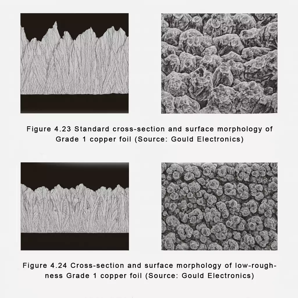
As operating frequencies increase, the impact of copper foil roughness on signal transmission performance becomes more pronounced. Due to the skin effect, high-frequency signals primarily travel along the surface of the conductor. The rougher the surface, the more distorted and extended the signal path becomes, resulting in greater signal attenuation.
As a result, low-profile copper foil is commonly used in high-speed and high-frequency PCBs to minimise signal loss, while still maintaining strong adhesion to high-performance resin systems.
Surface Treatment Processes for Copper Foil
After the electro-deposited copper foil is manufactured, it is typically subjected to surface treatments tailored to its end-use environment. These treatments enhance adhesion, oxidation resistance, and thermal stability. The most common surface treatment methods fall into four categories:
1. Nodular Treatment
This involves electroplating copper nodules or copper oxide nodules onto the foil surface to increase its surface area and improve bonding with resin systems.
Although the treatment layer is thin, it significantly enhances adhesion to high-performance resins such as polyimide, cyanate ester, or BT resin.
The matte surface shown in Figures 4.23 and 4.24 includes this type of spherical nodular structure.
2. Barrier Layer Treatment
A zinc, nickel, or brass alloy coating is applied to the honeycomb-like structure of the copper surface.
This barrier layer protects the resin-to-copper bond from deterioration during lamination or assembly, especially under heat or chemical exposure.
The typical thickness is several hundred angstroms (Å), and the colour varies depending on the metal type—commonly brown, grey, or mustard yellow.
3. Passivation & Anti-oxidation Layer
This treatment is usually applied to both sides of the copper foil to prevent oxidation during storage or lamination.
It typically consists of chromate compounds or organic anti-oxidation coatings.
These coatings are generally thinner than 100 Å and are removed during early PCB processing steps such as cleaning, etching, or scrubbing.
4. Coupling Agent Treatment
Silane-based coupling agents are applied to enhance chemical bonding between the copper foil and the resin system while preventing oxidation and surface contamination.
In certain high-performance substrate systems, silane treatment also improves bonding between the copper and glass fibre reinforcement.
Conclusion
Copper foil is the primary conductor in PCBs, and its properties directly affect board reliability and signal quality. By controlling the electrolytic process, grain structure, and surface roughness, you can optimise ductility and adhesion.
In high-density and high-speed designs, using HTE copper and low-roughness copper helps reduce cracking and signal loss. Selecting the right copper type and surface treatment strikes a balance between reliability and high-frequency performance, providing a stable conductive foundation for high-performance PCBs.
