


Rapid advances in modern electronics drove the emergence and evolution of Surface Mounting Technology (SMT). In recent decades, electronic applications have shown three defining trends: intelligent processing, multimedia integration, and networking.
Intelligent processing converts analog signals into digital form and enables computer-based control; multimedia integration extends communication beyond text to include sound and images, making electronic products more intuitive and pervasive; and networking connects formerly independent systems through high-speed, high-frequency data exchange, enabling global resource sharing.
These developments have imposed new demands on circuit-assembly technology: higher density, higher speed, and greater standardization.
- High density means handling more data in the same space.
- High-speed demands faster signal processing and data transfer.
- Standardization follows the industry's shift from a few mass-produced models to a more diverse, small-batch manufacturing approach. This approach requires consistent component design and assembly methods.
Evolution of SMT
SMT originated from hybrid-circuit manufacturing and has progressed through three major stages since the 1970s.
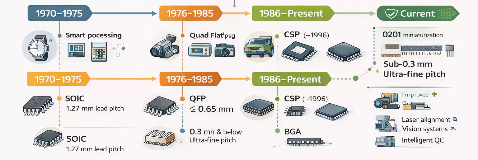
- 1970 – 1975:
The initial goal was to apply miniaturized chip components to hybrid (thick-film) circuits. SMT at this stage greatly advanced integrated-circuit (IC) fabrication techniques and first appeared in consumer products such as quartz watches and electronic calculators. - 1976 – 1985:
This period brought rapid miniaturization and multifunctionality. SMT was widely used in video cameras, pocket radios, and electronic still cameras. Automated surface-mount assembly equipment was introduced, and both process and material technologies matured, laying the foundation for high-volume production. - 1986 – present:
From 1986 onward, cost reduction and performance-to-price ratio became priorities. As process reliability improved, SMT expanded to military, automotive, computing, and industrial electronics. Automated placement and soldering systems became widespread. This further reduced overall manufacturing cost.
Co-development of Components and Technology
A key factor in SMT’s progress has been the parallel evolution of surface-mount components (SMC/SMD). The two are inseparable—the process's capability depends on the components available, and component design evolves with advances in assembly technology.
- During the 1960s, Philips (Europe) developed a button-type micro-device for watches that evolved into today’s Small Outline IC (SOIC) with gull-wing leads spaced at 1.27 mm and up to 28 pins.
- In the 1970s, Japanese manufacturers adopted the Quad Flat Package (QFP) for calculators, featuring gull-wing leads on all four sides, with spacing as fine as 0.65 mm and pin counts reaching several hundred.
- U.S. companies introduced the Plastic Leaded Chip Carrier (PLCC). Its 'J-shaped' leads resist deformation and minimize the mounting area. At the same time, Leadless Ceramic Chip Carriers (LCCC) used metallized pads instead of leads. This design allowed fully sealed ceramic packaging.
As a result, the assembly pitch narrowed from 1.27 mm to 0.65 mm, and eventually to 0.3 mm or below. By the early 1990s, fine-pitch SMT and its supporting equipment had reached maturity.
The Chip-Scale Package (CSP) emerged. It offered nearly equal chip and package sizes, low manufacturing cost, and compatibility with conventional IC testing. Around 1996, CSPs entered limited commercial production.
To handle growing I/O counts in highly integrated circuits, manufacturers adopted Ball Grid Array (BGA) devices. These used solder-ball interconnects are arranged across the entire underside of the package.
Modern SMT continues to improve the mounting of BGA and CSP packages. It also pushes toward sub-0.3 mm ultra-fine-pitch capability.
The miniaturization of surface-mount components has continuously driven advances in assembly technology. In turn, gains in assembly density and precision have set new requirements for component design. This creates a cycle in which progress in one area drives progress in the other.
Extension to Advanced Packaging
The 1990s saw the rise of the Multi-Chip Module (MCM)—a sophisticated hybrid circuit that integrates multiple bare ICs on a single substrate within a single enclosure. Compared with conventional SMT assemblies, an MCM can reduce area by three to six times and weight by more than threefold.
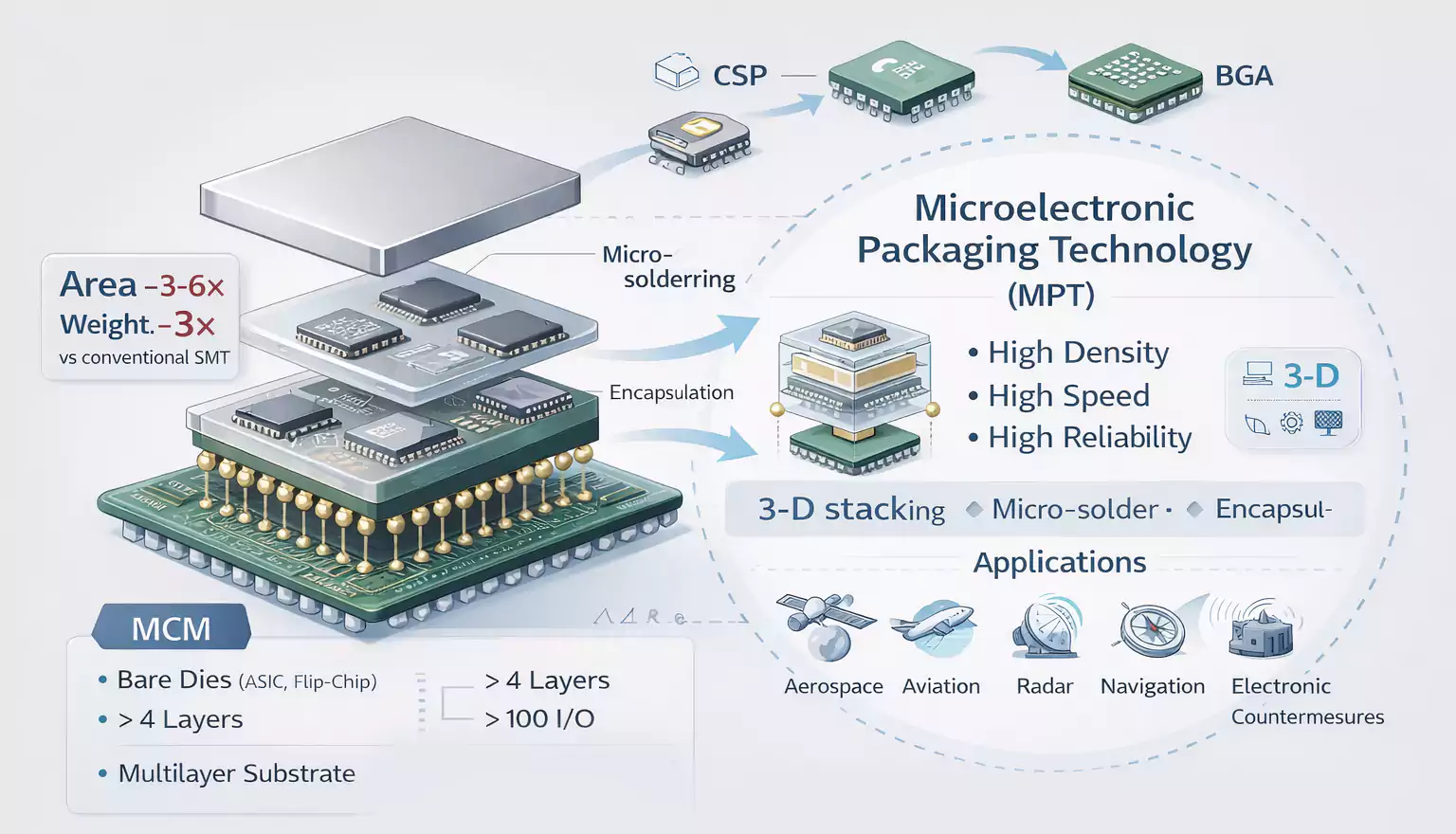
MCM technology extends SMT by combining semiconductor integration,thick- and thin-film hybrid microelectronics, and multilayer PCB fabrication. Typical MCM substrates use more than 4 wiring layers and over 100 I/O pads to connect chips such as ASICs, flip-chips, or custom CS devices. These modules represent the state of the art in 1990s packaging and are widely applied in supercomputers and aerospace electronics.
To meet demands for even higher density and multilayer interconnects, SMT has evolved. This field is now known internationally as Microelectronic Packaging Technology (MPT).
Centered on MCMs and 3-D stacked assemblies, MPT uses micro-soldering and encapsulation on dense, multilayer PCBs. This produces compact, high-speed, and highly reliable electronic subsystems.
MPT has become an essential branch of modern microelectronics. It plays a critical role in aerospace, aviation, radar, navigation, electronic countermeasures, and anti-interference systems.
Current Status and Significance
After more than forty years of evolution, SMT has reached full maturity and established itself as the fourth generation of electronic interconnection technology. It is now the mainstream approach worldwide for circuit assembly.
The general trend continues toward smaller components, higher mounting density, and greater process complexity. Ongoing progress focuses on four main areas:
- Miniaturization—mass adoption of 0201 (0.6 × 0.3 mm) components and fine-pitch QFP/BGA/CSP/flip-chip devices demands ultra-precise placement and alignment.
- Reliability—research addresses thermal-stress mismatches between materials, which can cause board cracking or solder-joint failure under harsh environments.
- Equipment innovation—modern SMT lines feature high-resolution laser alignment, optical vision systems, and intelligent quality-control tools for faster, denser, and more accurate assembly.
- Flexible PCB mounting—the industry has solved the challenge of rigidly fixing flexible substrates to ensure precise positioning during component placement.
SMT is vital to contemporary electronics manufacturing. It supports miniaturization, light weight, high performance, and reliability in today’s and tomorrow’s electronic products. This includes everything from consumer devices to defense and aerospace systems.
