

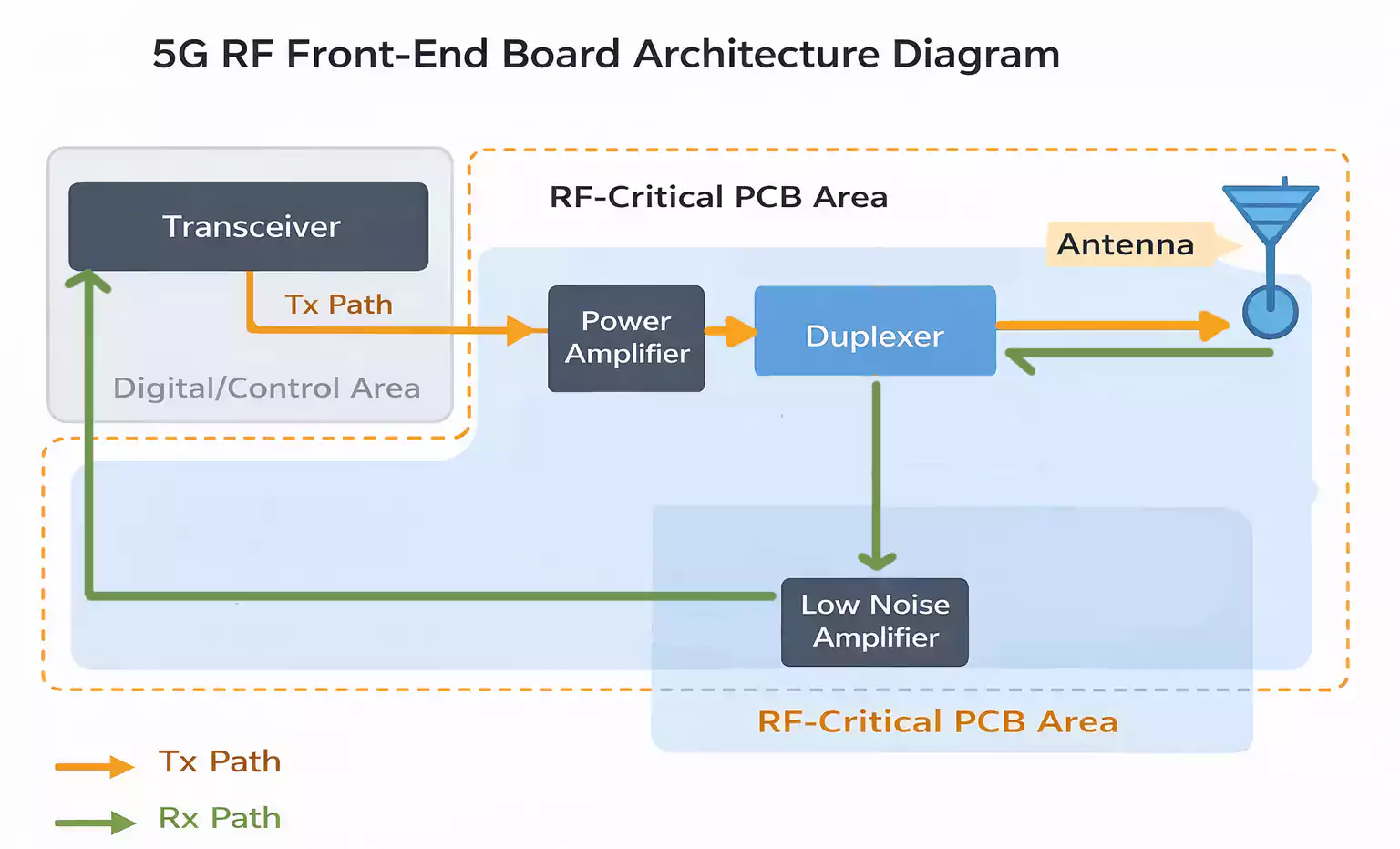


When layout and routing are complete, long-term reliability depends on a few practical PCB design guidelines: choosing manufacturable parts, selecting the right substrate, controlling EMI/EMC, and implementing a robust PCB thermal design. This Part 2 guide summarizes proven rules for U.S. manufacturing expectations and real-world production.
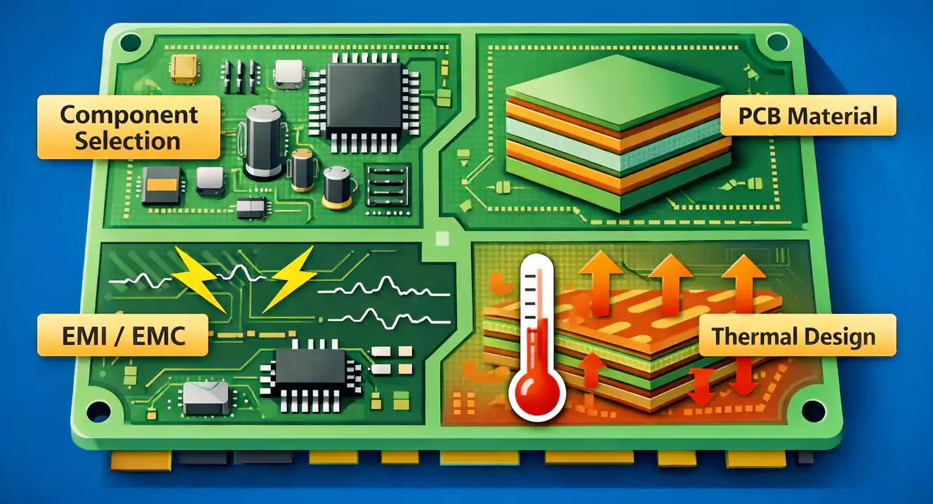
1. Component Selection: Think Beyond Size and Specs
Picking parts is not just an electrical decision. It’s also about assembly yield, inspection, rework risk, and cost.
Use mainstream packages when you can
Choosing the smallest package “just because it fits” can raise placement difficulty and increase failure risk. Standard footprints are typically easier to source, assemble, and verify.
Package choice matters: fine-pitch QFP needs caution.
For leaded ICs, lead shape and pitch drive both routing difficulty and soldering robustness. As a rule of thumb, QFP packages with a pitch below 0.5 mm warrant extra scrutiny. If the design allows it, a BGA option may be the more production-friendly route for dense I/O.
Check solderability and lead-free process tolerance.
Make sure the component’s packaging, terminal geometry, and reliability ratings align with your process window—especially if you run lead-free reflow.
Maintain a usable component library.
A disciplined library (mechanical outlines, pad dimensions, supplier info) reduces footprint mistakes and keeps manufacturing consistent across revisions.
2. PCB Material Selection: Match the Substrate to the Job
“FR-4” isn’t a single thing. Material classes differ significantly in electrical behavior, thermal stability, and long-term durability. Start by mapping requirements to structure—single-sided, double-sided, or multilayer—then confirm thickness based on board size and component loading.
Electrical needs come first.
If your design is sensitive to loss or impedance behavior, choose materials that support signal integrity requirements—not just what’s cheapest or familiar.
The reliability trio: Tg, CTE, and flatness
When boards see repeated thermal cycling, material properties become make-or-break:
- Tg (glass transition temperature): higher Tg typically supports better thermal robustness
- CTE (coefficient of thermal expansion): mismatch drives stress, especially through the Z-axis
- Flatness/warpage: affects assembly yield and inspection
Also pay attention to the board’s ability to support robust via formation and plated through-hole metallization, which is closely tied to reliability in multilayer builds.
Don’t ignore cost—balance it correctly.
Material pricing can vary widely across standard FR-4, high-Tg variants, polyimide, and RF laminates. Pick the lowest-cost option that still meets electrical and reliability needs.
3. EMI / EMC: Reduce Coupling Before It Becomes a Problem
External interference can be addressed with enclosure shielding and circuit hardening, but board-generated noise is largely determined by how you place and route things.
Separate noisy and sensitive zones
If two parts can interfere with each other, distance is your first tool. When distance isn’t possible, isolation or shielding becomes necessary.
Avoid long parallel runs across different “frequency worlds.”
Running unrelated signals in parallel can lead to crosstalk. For fast or high-frequency traces, a grounded shield/guard line can help when used appropriately.
Use the stack-up to your advantage.
- On two-layer boards, dedicate one side to signals and keep the other as a continuous ground reference when possible.
- On multilayer designs, placing susceptible traces between solid reference layers can reduce both radiation and pickup.
- For microwave-style routing, the transmission structure and dielectric thickness must meet the impedance target.
Keep high-frequency paths short.
Shorter transistor base runs and shorter high-frequency routes generally mean less radiated energy and fewer opportunities for coupling.
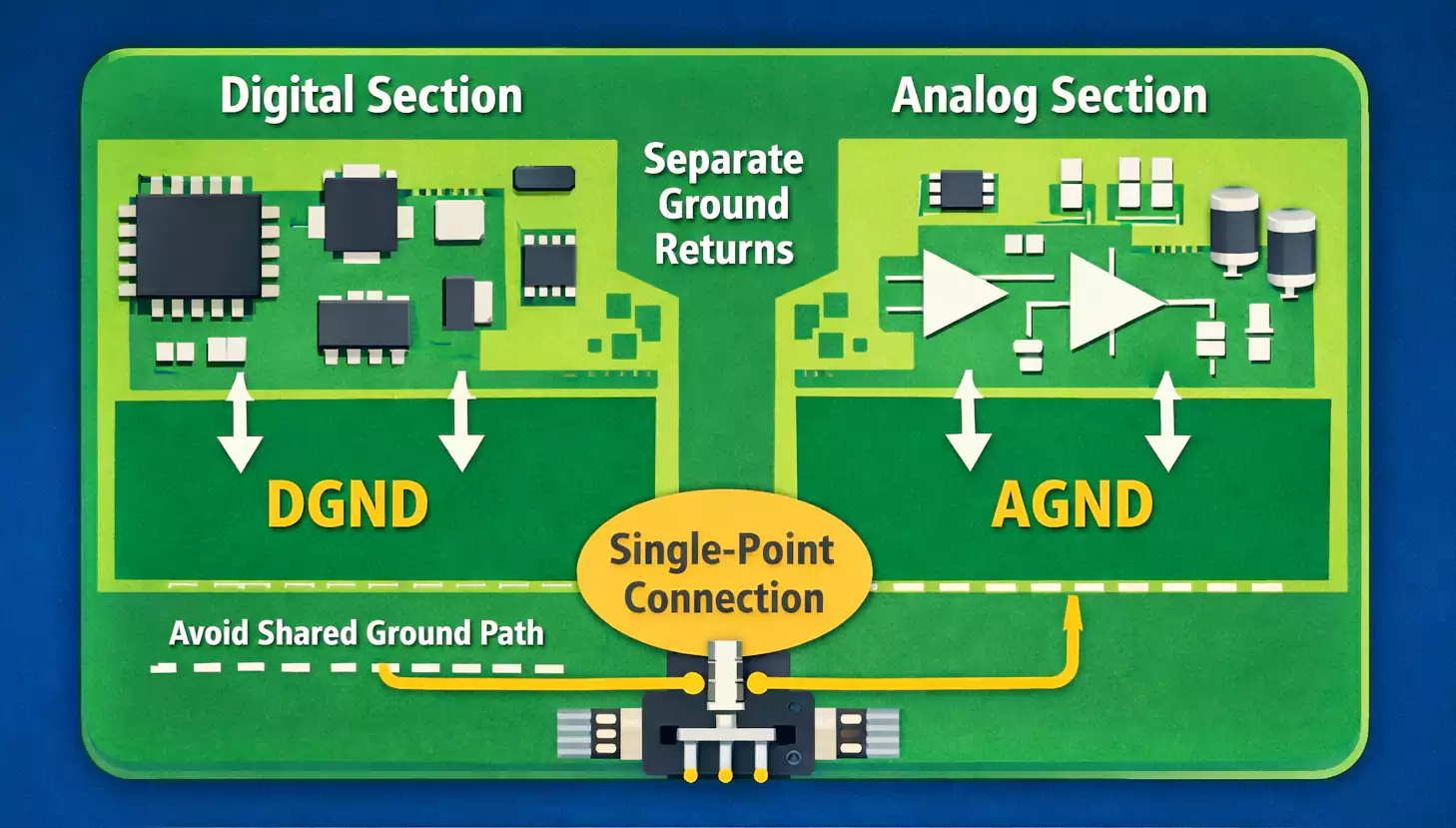
Separate return paths and power/ground domains when frequencies differ
Sharing the same ground/power routing across different frequency circuits is a common source of noise injection.
Split analog and digital ground—then join once
A practical approach is to keep analog and digital ground systems separate, then connect them at a single common point at the external ground interface.
Increase spacing where voltage differences are large
More distance reduces coupling and lowers risk under stress.
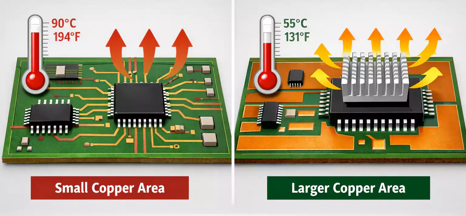
4. Thermal Planning: Don’t Let Heat Set Your Limits
As density rises, temperature becomes a reliability driver. Excess heat can shift parameters, reduce lifetime, and trigger outright failures.
Use copper as a heat spreader.
More copper area around high-power parts—especially on the ground—helps distribute heat and reduce hot spots.
Add mechanical help when required.
High-dissipation components may need to be raised off the board or paired with heatsinks to prevent heat from concentrating in the laminate.
Internal ground as mesh (and edge-aware design)
For multilayer boards, a mesh-style internal ground pattern and edge-aware placement can enhance structural strength and improve thermal performance.
Select heat-resistant/flame-retardant materials when needed.
If the environment or process temperature is demanding, choose materials that can withstand it.
Takeaway
These PCB design guidelines—strong PCB component selection, correct PCB material selection, disciplined EMI/EMC control, and practical PCB thermal design—help reduce rework, improve manufacturability, and increase long-term reliability in production.
