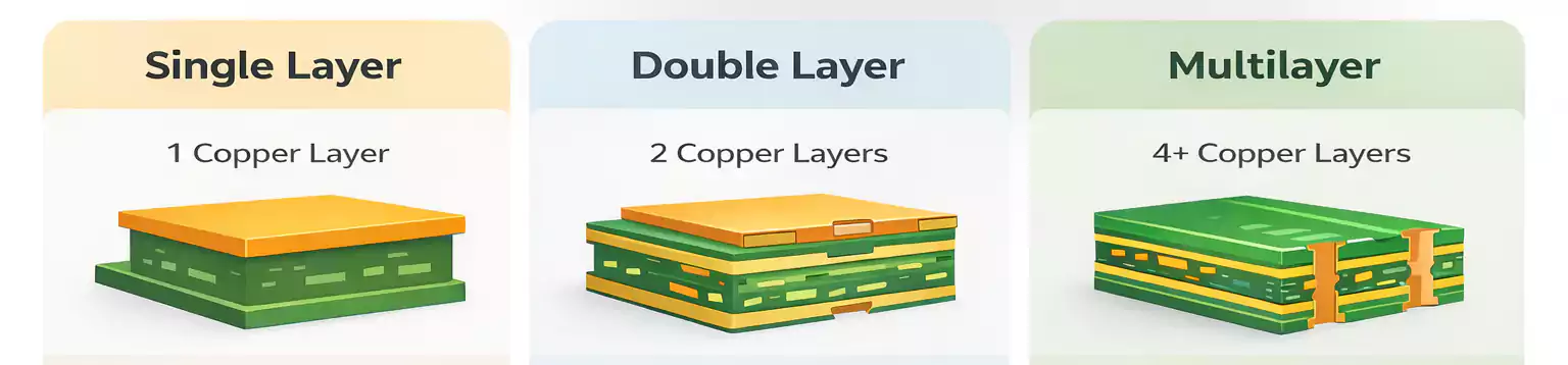
A multilayer PCB (also called a multilayer PCB board) is a printed circuit board with three or more copper layers, stacked together with insulating dielectric materials and laminated under heat and pressure. While double-sided PCBs can support moderate complexity, modern electronics—especially wireless systems, compact consumer devices, and high-speed digital equipment—require far more routing density, improved EMI performance, and better power integrity.
This guide explains what multilayer PCBs are, how layer counts are selected, essential multilayer PCB design principles, the manufacturing workflow, and common use cases.
What Is a Multilayer PCB?
A multilayer PCB is built from alternating copper foils and dielectric prepreg or core materials, laminated into a single, rigid structure. The outer layers (Top and Bottom) typically host components, while inner layers are reserved for routing, power distribution, and ground reference planes.
How it differs from a double-sided PCB
| Routing density | Moderate | Very high |
| Signal integrity | Limited | Excellent (due to reference planes) |
| EMI control | Basic | Strong, predictable |
| Size reduction | Limited | Significant |
| Cost | Low | Higher |
| Reliability | Good | Excellent (shorter traces, lower noise) |
While a double-sided PCB routes signals only on two layers, a multilayer board provides multiple internal routing channels, enabling designers to achieve compact layouts, short return paths, and controlled impedance for high-speed interfaces.
How to identify a multilayer PCB
A quick visual test is the edge profile—multilayer PCBs show multiple laminated layers instead of a single uniform core. High-density boards also feel slightly heavier due to the additional copper.
Anatomy of a Multilayer PCB
A typical multilayer PCB resembles a copper-and-dielectric sandwich:
- Top Layer – component pads, short routes
- Internal Signal Layers – controlled routing, dense nets
- Power Plane Layers – low-impedance power delivery
- Ground Plane Layers – reference plane for all signals
- Bottom Layer – components, connectors, or breakout routing
Dielectric materials maintain spacing and determine key electrical properties, such as impedance, loss, and crosstalk behavior. Thinner dielectrics and tighter coupling to ground help improve high-speed performance.
How Many Layers Do You Need?
Most commercial multilayer PCBs range from 4 to 12 layers, though networking, automotive radar, and server computing systems often require 16–30+ layers.
Why do most multilayer PCBs use an even number of layers?
Even-layer constructions laminate more evenly, reducing the risk of warpage and improving manufacturing yield. Odd-layer boards are possible but generally discouraged due to increased stress and cost.
Quick decision guide
| Basic MCU, IoT, power-sensitive boards | 4-layer |
| Medium-complexity digital designs, RF sections | 6-layer |
| High-speed interfaces (USB 3.x, PCIe, DDR), moderate density | 8-layer |
| Very dense systems, multiple BGAs, controlled impedance + EMC | 10–12 layers |
When choosing layers, consider:
- BGA pitch & I/O count
- High-speed signals requiring adjacent reference planes
- Number of power rails
- Stackup symmetry and manufacturability
- Cost vs. performance requirements
Via Types: Through-Hole, Blind, and Buried
Multilayer PCBs rely on vias to interconnect layers. The most common types include:
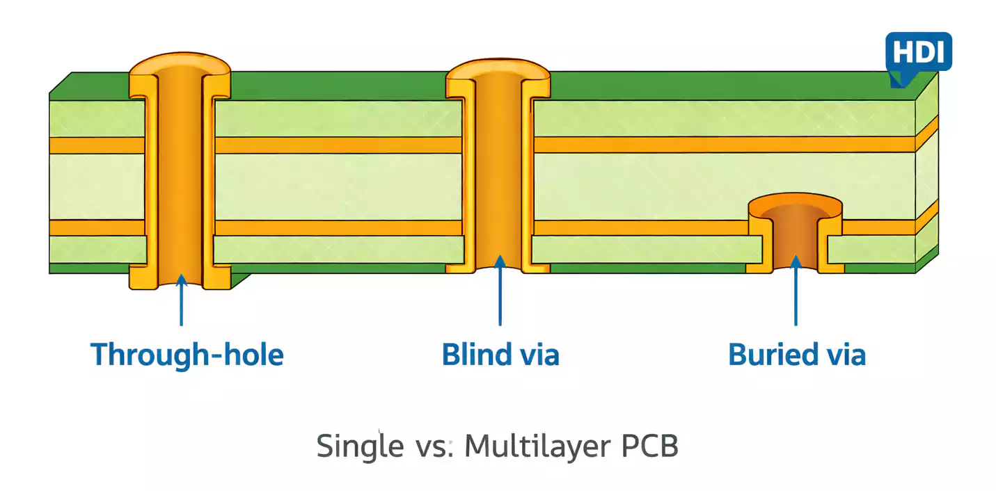
1. Through-Hole Via (PTH)
- Drilled from top to bottom
- Lowest cost and simplest to fabricate
- Suitable for general routing and component leads
2. Blind Via
- Connects an outer layer to one or more inner layers
- Avoids routing congestion under dense BGAs
- Costs more due to precise depth control
3. Buried Via
- Connects only internal layers
- Frees up surface area for routing
- Often used in compact/high-speed designs.
A note on HDI multilayer PCBs
High-density interconnects (HDI) use microvias—laser-drilled tiny vias that support extremely tight BGA pitches and short signal paths.
Multilayer PCB Design Essentials
This section summarizes the practical, widely applicable design rules that engineers should follow when designing multilayer boards.
1. Stackup design fundamentals
A good stackup is the backbone of a reliable multilayer PCB. Three essential guidelines:
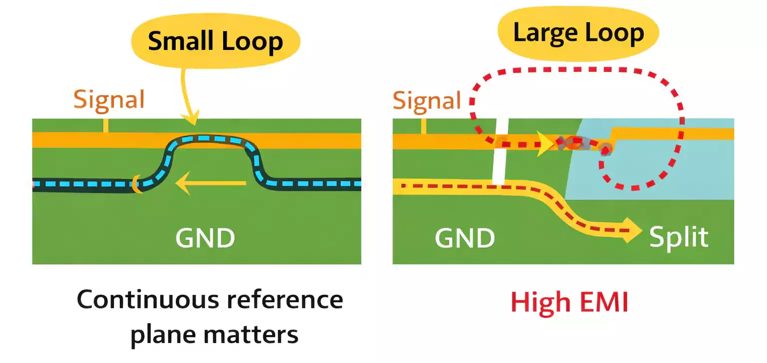
Rule 1: Keep signal layers adjacent to ground or power planes
This ensures tight electromagnetic coupling, minimizing loop area and improving signal integrity.
Rule 2: Maintain a continuous return path
High-speed signals always seek the path of least inductance. Avoid crossing split planes, as they disrupt the return path and cause EMI problems.
Rule 3: Preserve stackup symmetry
Uneven copper distribution leads to bowing or twisting during lamination. A symmetrical structure minimizes mechanical stress.
2. Using power and ground planes
Dedicated ground and power planes:
- Reduce noise
- Improve power integrity
- Enable predictable controlled-impedance routing.
On digital boards, designers often place GND planes centrally to improve shielding between signal layers.
3. Routing guidelines for high-speed and mixed-signal boards
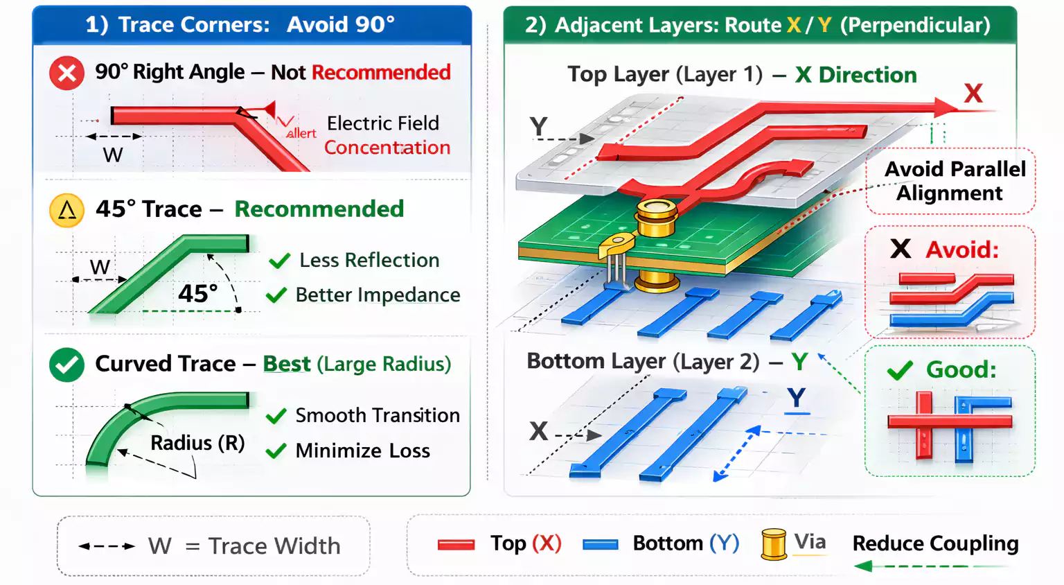
- Minimize layer transitions to reduce via stubs and reflections.
- Route adjacent layers orthogonally (X–Y routing) to reduce crosstalk
- Maintain consistent reference planes under differential pairs.
- Keep clocks and high-speed lines away from noisy power circuits.
- For sensitive analog sections, isolate switching return currents.
These are broad, high-value rules applicable across industries without going deep into niche calculations.
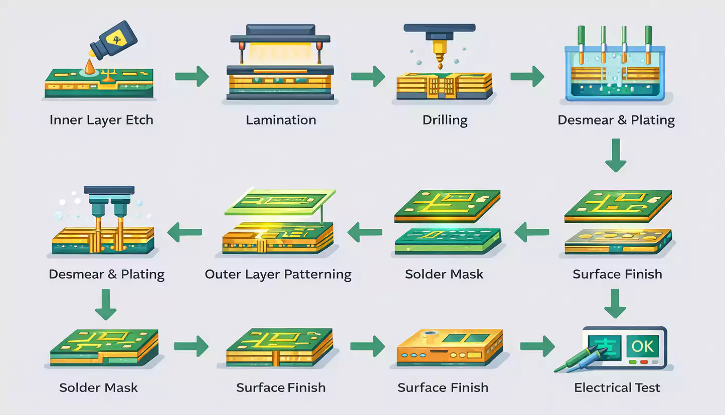
Multilayer PCB Fabrication: The Manufacturing Workflow
Multilayer PCB fabrication follows a structured, step-by-step sequence. Below is an accessible overview of what happens in the factory.
Step 1: Inner layer imaging & etching
Copper is laminated with photoresist, patterned with UV exposure, and etched to form the board's internal circuits.
Step 2: Lamination
Multiple cores and prepreg layers are pressed together at high temperature and pressure, forming a solid multilayer stack. This step requires precise control to avoid voids, misregistrations, or warpage.
Step 3: Mechanical drilling
Thousands of holes are drilled for vias and component leads. Drill quality affects plating reliability and annular ring accuracy.
Step 4: Desmear & copper plating
Resin left from drilling is removed (“desmear”), and the hole walls are plated with copper. This creates electrically conductive barrels, which are essential for multilayer interconnections.
Step 5: Outer layer patterning
After lamination, outer layers undergo imaging and etching to form the top and bottom routing features.
Step 6: Solder mask & silkscreen
Solder mask protects copper features from oxidation and solder bridging. Silkscreen adds component labels and polarity markings.
Step 7: Final finishing
Surface finishes such as HASL, ENIG, ENEPIG, or OSP are applied to exposed copper pads to prepare them for assembly.
Step 8: Electrical & functional testing
Flying-probe or bed-of-nails tests verify continuity, shorts, and correct layer connectivity.
Advantages and Disadvantages of Multilayer PCBs
Key advantages
- High routing density → supports compact product designs.
- Improved EMI/EMC performance
- Better signal integrity due to dedicated reference planes
- Shorter traces → lower parasitics, reduced noise
- Stronger mechanical stability compared to single-layer boards.
Key limitations
- Higher manufacturing cost than simpler boards
- More complex design and layout requirements
- Troubleshooting and rework are harder due to buried structures.
Despite these tradeoffs, multilayer PCBs remain the preferred foundation of modern electronics.
Common Applications of Multilayer PCBs
Multilayer PCBs appear in nearly every advanced electronic device, including:
- Consumer Electronics
Smartphones, laptops, tablets, wearables, cameras
- Communication Equipment
Routers, base stations, RF modules, satellite electronics
- Industrial & Automation
Motor drivers, PLCs, instrumentation, sensor interfaces
- Automotive & Transportation
ADAS modules, radar systems, infotainment, EV control units
- Medical Devices
Portable monitors, imaging systems, and handheld analyzers
Their ability to support high functionality in minimal space makes multilayer PCBs indispensable across these industries.
Frequently Asked Questions (FAQ)
What is the minimum number of layers in a multilayer PCB?
Three copper layers are the technical minimum, but 4-layer PCBs are the most commonly produced “true” multilayer designs.
Why are most multilayer PCBs built with an even number of layers?
Even-layer boards laminate more uniformly, reducing mechanical stress and manufacturing defects.
When should I choose a 4-layer vs. 6-layer PCB?
Choose 4 layers for basic IoT/microcontroller projects; 6 layers when routing complexity or EMI requirements increase.
What’s the difference between blind, buried, and through-hole vias?
·Through-hole: top to bottom
·Blind: outer layer to inner layer
·Buried: inner-to-inner layer only
Why do multilayer PCBs offer better EMI performance?
Signals can be routed on continuous copper planes, reducing loop area and minimizing radiation.
What makes multilayer PCBs harder to repair?
Internal layers cannot be accessed directly, and faults may be buried between dielectric layers.
How do you tell if a PCB is multilayer?
Check the board edge—multiple laminated layers will be visible.
Final Thoughts
Multilayer PCBs form the backbone of modern, high-performance electronics. By understanding layer selection, stackup design, routing fundamentals, and multilayer fabrication, engineers can create more reliable, compact, and EMI-robust products.
If you are looking for high-quality multilayer PCB fabrication, FastTurnPCB specializes in fast turnaround, advanced stackups, and dependable engineering support for prototypes and production volumes.