

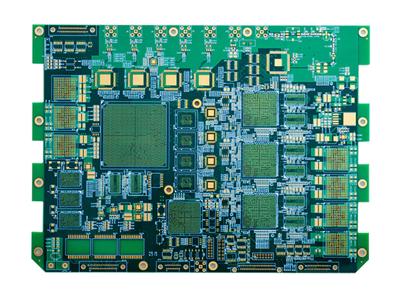
In high-density PCB design, the most direct way to increase functionality is to place more traces in a limited area.
However, higher routing density is not only a layout challenge — it also depends on how copper foil materials have improved over time.
As multilayer, HDI, and thick PCBs become more common, copper foil has changed from a simple conductor into a critical engineering material that affects reliability, yield, and product lifetime.
This article reviews the main types of copper foils used in modern PCBs and explains how each one supports manufacturing quality and structural reliability.
1. Why Copper Foil Matters in High-Density PCBs
In the PCB industry, copper foil is usually classified by the IPC-4562 standard. Among these types, Electrodeposited (ED) copper foil is the most common in multilayer and HDI designs.
As traces narrow, layer counts increase, and boards get thicker, standard copper foil can no longer stretch enough at high temperatures or during thermal cycles.
This problem led to the development of HTE (High Temperature Elongation) copper foil.
Besides HTE copper, low-roughness foils, Reverse Treated Foil (RTF), and foils made for high-performance resin systems are now standard options in advanced PCB design.
2. HTE Copper Foil – The Base for Thermal Reliability
According to IPC-4562, HTE copper foil is typically listed as Grade 3.
Compared with standard electrodeposited copper (Grade 1), HTE foil has much better elongation at high temperatures.
At 180 °C, its elongation is typically between 4% and 10%.
This property is very important in multilayer boards.
During reflow soldering or long thermal cycles, the dielectric expands along the Z-axis.
This expansion adds stress at the joint between the inner-layer copper and the plated-through hole (PTH).
If the foil cannot stretch, it can crack or separate, leading to interconnect failure.
HTE copper helps absorb this stress through higher plastic deformation.
It improves reliability in conditions such as:
- Thick board designs
- Laminates with high resin content
- Applications with large thermal cycling stress
In real projects, elongation at 180 °C, tensile strength, and peel strength are the main parameters engineers look at when choosing HTE copper.
3. Low-Roughness Copper Foil – For Fine Lines and Impedance Control

As line width and spacing get smaller, the surface profile of copper becomes a key factor in line quality.
Standard-roughness copper has visible surface nodules, often called copper teeth.
These cause several issues during fine-line etching:
- Distorted trace geometry
- Uneven dielectric thickness in thin laminates
- Difficult impedance control
In extreme cases, large copper teeth on both sides of the dielectric can cause unstable geometry or impedance, and even lead to electrical failure, such as lower arc resistance (Arc Resistance).
For this reason, low-roughness copper foil is now essential for precise lines and consistent impedance.
Roughness is usually measured by Ra, Rz, or Sq.
Among these, Rz and Sq better describe the height and distribution of copper nodules, which matter most for fine lines.

4. RTF Copper Foil – Balancing Adhesion and Smoothness
Reverse Treated Foil (RTF) is an improved version of low-roughness copper foil.
During electrodeposition, copper foil naturally forms two surfaces — a smooth, shiny side and a rough, matte side.
Traditional foils are treated on the matte side, which is bonded to the dielectric.
RTF foils are treated on the shiny side and then laminated to the dielectric.

This design gives two clear benefits:
- The treated, shiny side provides very low surface roughness, which helps fine-line etching.
- The matte side faces outward, giving better adhesion for photoresist during imaging.
In some processes, RTF can reduce or even remove the need for inner-layer roughening steps, improving inner-layer imaging and etching yield.
That is why RTF is widely used in HDI and high-end multilayer PCBs.
5. Copper Foil for High-Performance Resin Systems – More Than Just Roughness
In resin systems such as BT resin, polyimide, cyanate ester, and some high-Tg epoxies, materials are more sensitive to corrosive chemicals during PCB manufacturing and long-term use.
This can lower peel strength and reduce durability.
To solve this, manufacturers often use two methods:
- Nodular treatment on copper foil to increase the mechanical bonding area.
- Coupling agents in the resin to create chemical bonds with copper.
In practice, both methods are used together to balance peel strength, chemical resistance, and thermal reliability — not just to make the surface rougher.
Conclusion
In high-density PCB design, copper foil is no longer just a conductive layer.
HTE, low-roughness, RTF, and resin-specific copper foils together form the foundation of reliability, yield, and manufacturability in modern PCB production.
