

Copper foil is the primary conductor material used in PCBs. The trend toward higher circuit density has driven new developments in copper foil technology. In addition, copper foil can be plated with other metal alloys to create embedded resistors inside multilayer PCBs.
1. Dull-Side Treated Foil (DSTF) or Reverse-Treated Foil (RTF)
DSTF/RTF are also types of electro-deposited (ED) copper foil, but RTF applies the treatment to the shiny side, not the rough side, as with standard ED foil (see Figures 4.25 and 4.26).
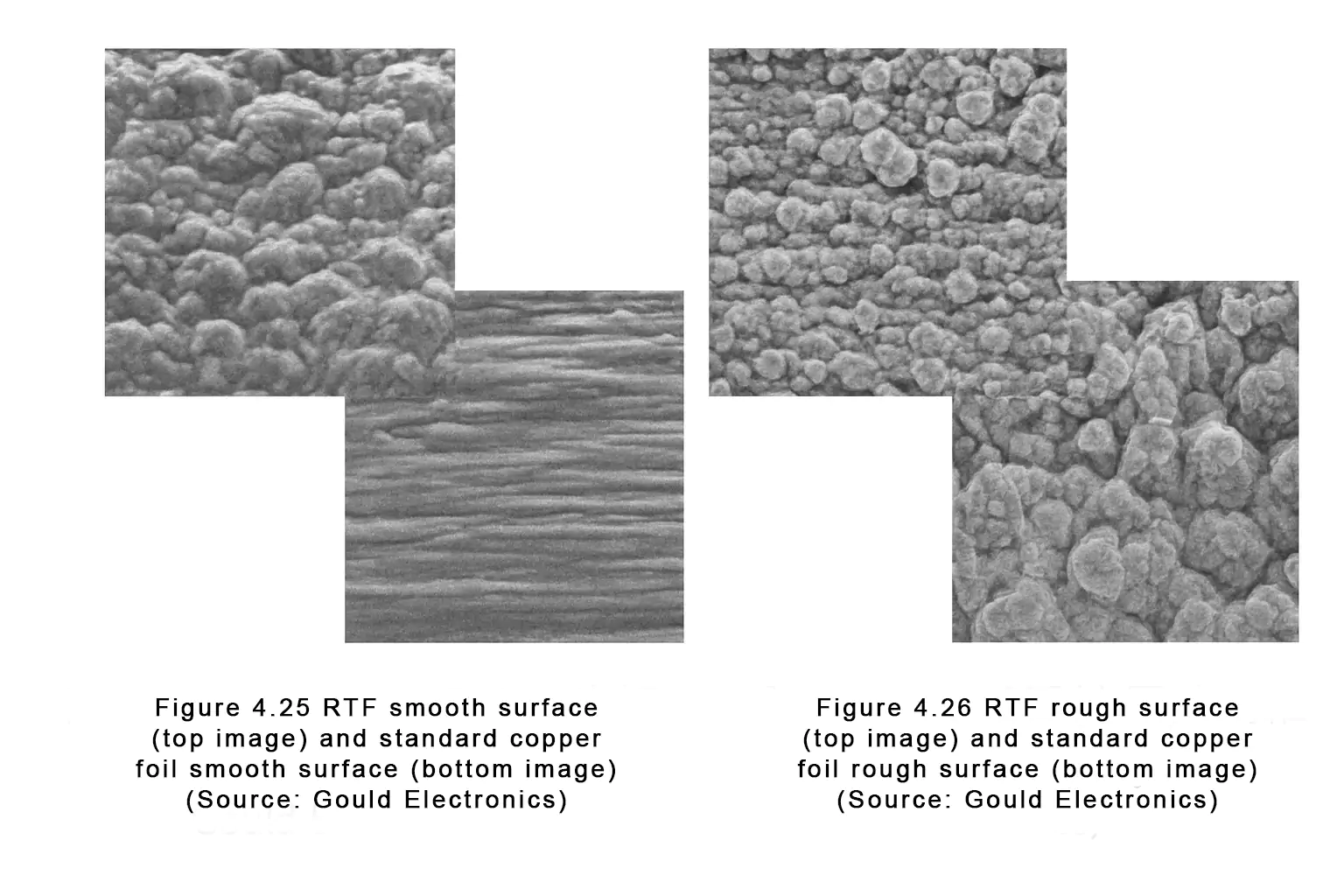
As a result, the side bonding to the resin has very low roughness, while the rough side faces outward. Low foil roughness on the laminate helps form fine inner-layer traces. The rough side still provides adhesion.
For high-frequency signals, the low-roughness surface offers much better electrical performance. For thin cores, low roughness also helps maintain uniform dielectric thickness and reduces “tooth” intrusion from copper peaks, which can improve dielectric breakdown strength. These benefits come with a slight reduction in peel strength.
2. Rolled-Annealed (RA) Copper Foil
Rolled-annealed copper foil has excellent ductility and is commonly used for flexible circuits. It is produced by hot-rolling thick copper sheet or ingot multiple times at high temperature to achieve the desired thickness and mechanical properties.

Compared with ED foil, RA foil has a more random grain structure, which results in superior mechanical properties. Both sides have low roughness, so you can choose either side for surface treatment.
3. Copper Foil Purity and Resistivity
IPC-4562, Metal Foil for Printed Wiring Applications, defines purity and resistivity for ED and RA foils.
The minimum purity of untreated ED copper foil is 99.8%, and the silver content is included in the copper content. RA copper foil has a purity of 99.9%.
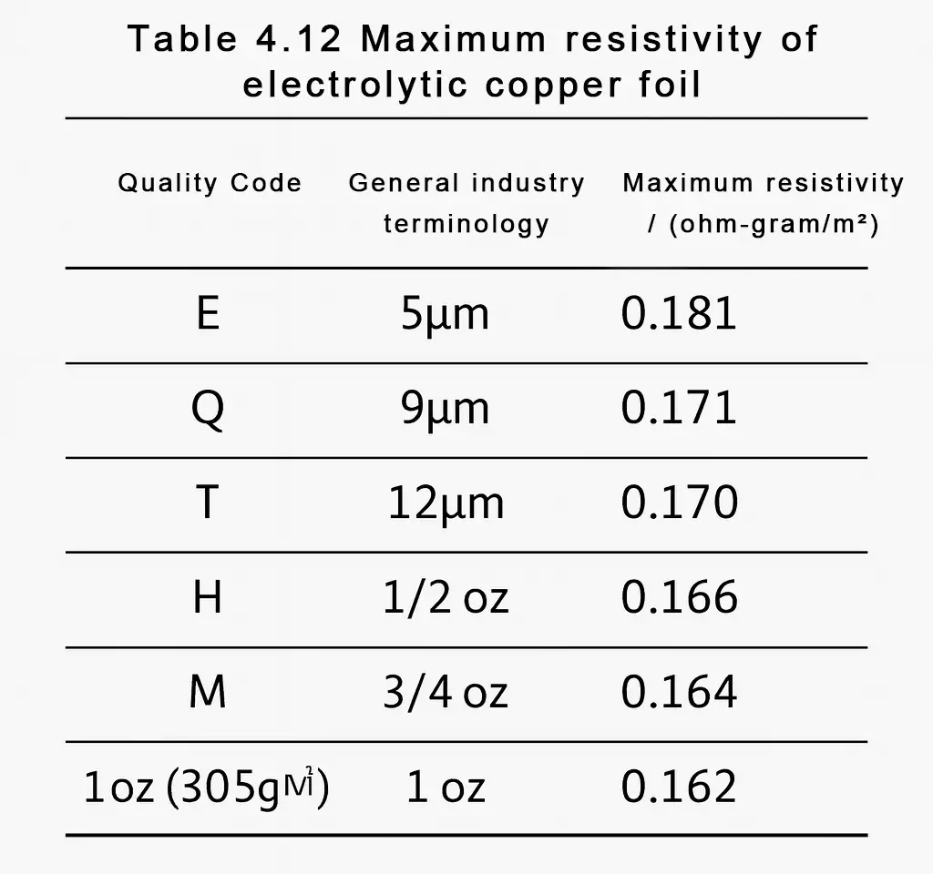
Table 4.12 gives the resistivity requirements for ED copper foil. The maximum resistivity of RA foil depends on foil quality and is generally 0.155–0.160 ohm-gram/m².
4. Other Copper Foil Types
Standard ED foils are suitable for most rigid and flexible PCBs. For special applications, modified foils are used, including double-treated foil, resistive foil, and ultra-thin ED foil.
① Double-Treated Foil
Both sides of the foil receive special surface treatments. The side contacting the substrate is treated to improve adhesion and reliability with the resin. The other side is “reverse-treated,” so the shiny side bonds to the substrate and the rough side faces outward.
It can eliminate steps such as inner-layer browning before lamination. However, it requires very high surface cleanliness, so it is used less often in PCB manufacturing.
② Resistive Copper Foil
Processing the base copper can form embedded resistors in the inner layer. This reduces the number of discrete resistors on the outer layers and builds resistors directly inside the multilayer board. It can improve reliability and free board space for active components.
These foils are typically made by coating a metal-alloy resistive layer on the base foil. Laminates made with this foil can then be patterned by photoimaging and etching to create resistor elements.
③ Ultra-Thin ED Foil
Ultra-thin ED foil, such as 2 μm foil, cannot be stored alone because it wrinkles easily and can be scraped. It is usually attached to a carrier foil. The carrier is thicker, such as 15 μm. After lamination, the carrier is removed.
This is used for ultra-fine-line PCBs and is primarily applied to packaging substrate materials.
Conclusion
Different copper foils have different strengths and use cases. ED foil has mature processes and excellent adhesion. RA foil offers high ductility, making it ideal for flexible circuits. As high-frequency and high-density designs grow, low-roughness, high-purity, and functional foils will be more critical. Choosing the right foil is key to PCB performance and reliability.
