


Introduction
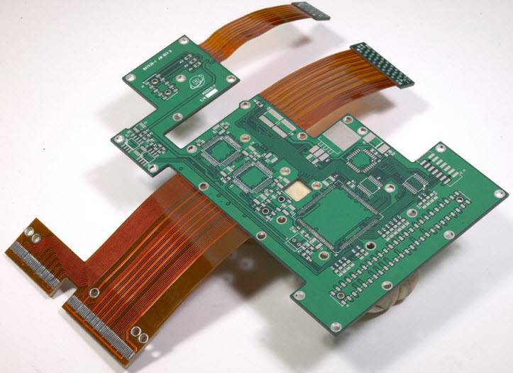
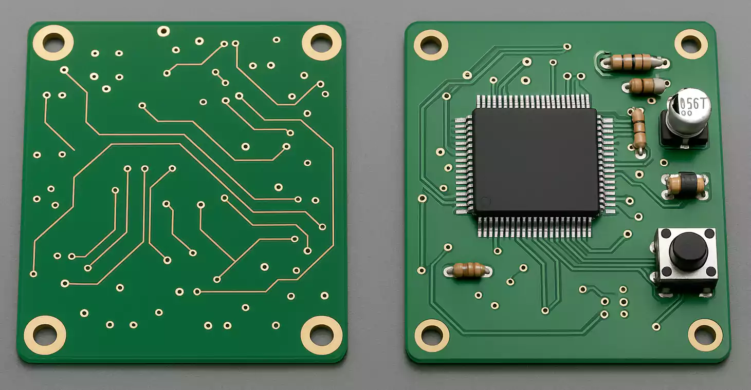
A blank PCB, also called a bare board, is the foundation of every electronic device—from smartphones and routers to power supplies and sensors. But a blank board by itself does nothing until it’s populated with the right parts and assembled into a PCBA (Printed Circuit Board Assembly).
This guide explains everything you need to know about Blank PCB and Parts—what they are, how they’re made, where to buy them, and how to go from a bare board to a functioning assembly step by step.
What Is a Blank (Bare) PCB?
A blank PCB is a circuit board without any components soldered on it. It provides the mechanical structure and electrical pathways that connect components together. Think of it as the skeleton of your electronic device.
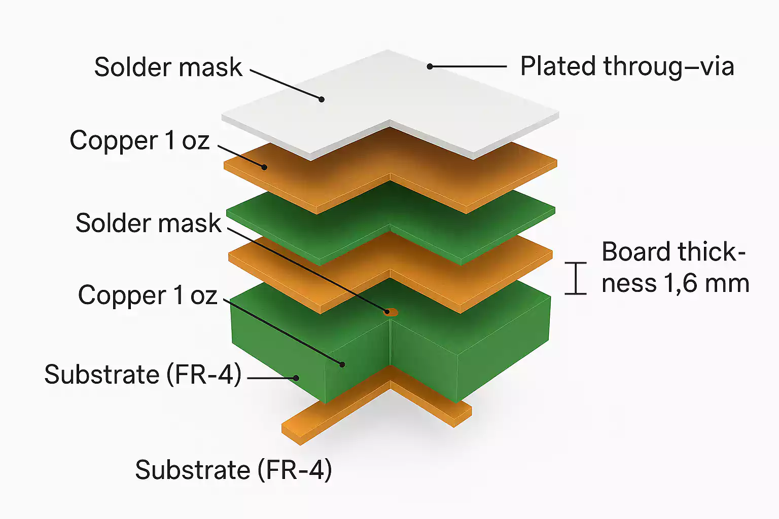
A typical blank PCB consists of several layers:
- Base material (substrate): Usually FR-4 fiberglass, known for strength and insulation.
- Copper layer: Conductive traces that form the circuits.
- Solder mask: The green (or other colored) coating that insulates copper and prevents solder bridges.
- Silkscreen: Printed labels showing component names and outlines.
- Vias and holes: Allow connections between layers or for through-hole parts.
Key specifications include layer count (1–16 or more), board thickness (commonly 1.6 mm), copper thickness (1–2 oz), and minimum trace/space (6 mil/6 mil).
When hobbyists mention “zero PCB” or “prototype board”, they often mean a perforated universal board with pre-drilled holes but no predefined copper traces. A blank or bare PCB, by contrast, has a specific circuit pattern designed for one project.
Blank PCB vs. PCBA: Don’t Confuse the Terms
It’s easy to mix these terms up.
- A PCB (Printed Circuit Board) is just the bare board.
- A PCBA (Printed Circuit Board Assembly) is the same board with electronic components soldered on.
In manufacturing, the flow goes like this: PCB → PCBA → Final Product.
You design and fabricate the PCB first, then assemble it with parts to build a working device.
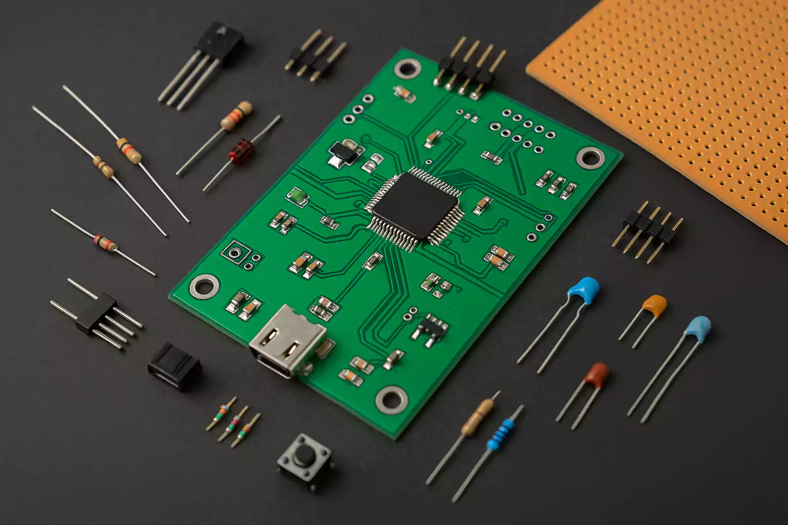
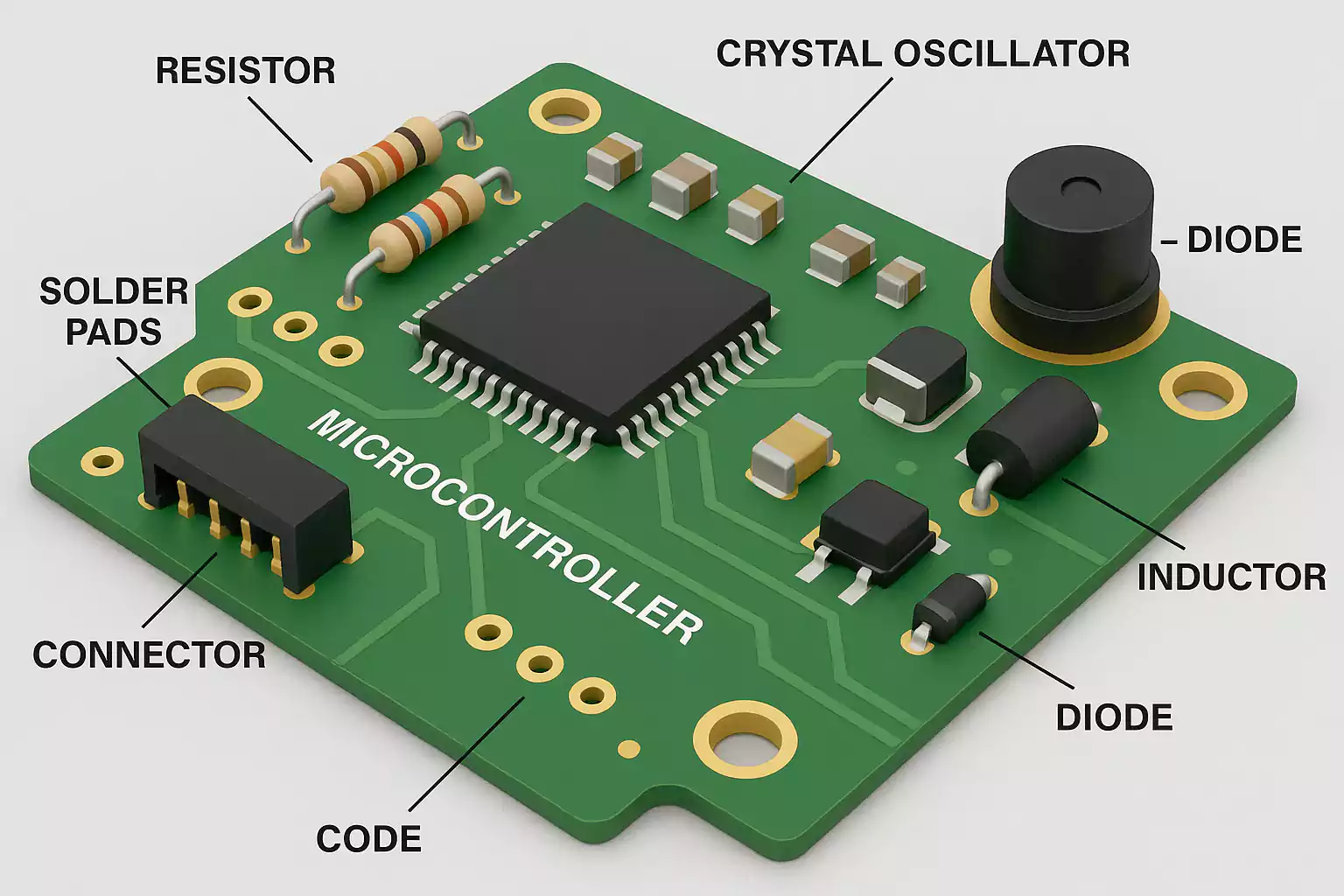
Blank PCB and Parts: What Components You’ll Need
A blank PCB becomes functional only after it’s populated with electronic parts. These parts fall into several categories:
1. Passive Components
These include resistors, capacitors, and inductors. They control voltage, filter noise, and shape signals. They don’t need power to operate but are essential for circuit stability.
2. Active Components
These are ICs (integrated circuits), transistors, voltage regulators, and diodes. Active parts amplify signals, switch currents, and perform logical functions.
3. Connectors
Connectors allow your board to communicate with the outside world—USB ports, pin headers, power jacks, or edge connectors.
4. Mechanical and Thermal Parts
Heatsinks, mounting holes, spacers, and screws fall into this category. They help with mechanical support and heat dissipation.
5. Interfaces and Debug Points
Programming headers, test pads, and jumpers are used during development and testing.
Through-hole vs. Surface-mount:
Components come in two main mounting styles. Through-hole (THD) parts have leads that go through drilled holes and are easy for beginners to solder. Surface-mount (SMD) parts sit directly on the copper pads—better for automated assembly and compact designs.
Example parts list for a simple project:
- DC power jack and voltage regulator
- Microcontroller (e.g., ATmega or STM32)
- Capacitors and resistors for filtering
- LEDs and pushbuttons
- Pin headers for inputs/outputs
- USB or serial connector for communication
Buying Blank PCBs and Parts: Cost and Sourcing Tips
Where to Buy Blank PCBs
You can easily order blank PCBs from trusted manufacturers that specialize in quick-turn prototype and small-batch production. They support instant online quotes, Gerber file uploads, and deliver high-quality boards within just a few days. Services include:
- Rapid prototypes (1–10 pieces) for engineers, makers, or students
- Small-volume manufacturing for startups or pilot runs
- Multiple material options such as FR-4, aluminum, and Rogers high-frequency laminates
- Free DFM checking, electrical testing, and custom finishes (ENIG, HASL, OSP)
Fast Turn PCBs combines speed, quality, and cost efficiency, making it a reliable choice for anyone needing blank PCBs fast.
2. Where to Buy Electronic Parts
Components can be purchased from:
- Authorized distributors: Mouser, Digi-Key, Arrow, etc. (quality and traceability guaranteed)
- Reseller platforms: Amazon, eBay, or maker suppliers (good for small projects, but watch for counterfeits)
- Local electronics stores for common resistors and capacitors.
3. Cost Breakdown
A basic cost structure looks like this:
- Blank PCB fabrication: Depends on board size, layers, copper thickness, and finish (HASL, ENIG).
- Components: Prices vary widely; bulk buying reduces cost.
- Assembly: Hand soldering for prototypes, SMT reflow or wave soldering for production.
- Testing: Functional and in-circuit testing add small costs but ensure reliability.
- Shipping and handling.
4. Lead Time Factors
- More layers or fine traces → longer production
- Special finishes (ENIG, immersion silver) → +1–2 days
- Out-of-stock parts → delays during assembly
For a small two-layer board, typical turnaround is 3–5 days for PCB fabrication and another 3–7 days for parts procurement and assembly.
From Blank to PCBA: The 7-Step Process
Turning a blank board into a working assembly involves careful planning and execution. Here’s the complete flow used by professionals and hobbyists alike.
Step 1: Create the Schematic and BOM
Start with an electronic design in software such as KiCad, Altium Designer, or EasyEDA. The schematic defines how each part connects.
Export a BOM (Bill of Materials) listing every component’s name, value, footprint, and quantity.
Choose parts that are readily available from distributors to avoid long lead times.
Step 2: PCB Layout Design
Translate the schematic into a board layout.
Define the stack-up (number of layers and copper thickness).
Route traces according to design rules: spacing, current capacity, and impedance control if needed.
Leave enough clearance for soldering and assembly—especially around connectors and tall components.
Step 3: Design for Manufacturability (DFM) Check
Before ordering your board, review manufacturability:
- Minimum trace width and spacing
- Drill size and via tolerances
- Solder mask clearances and openings
- Silkscreen legibility and reference placement
- Add fiducial marks for automated pick-and-place assembly
Many PCB manufacturers provide free DFM checking tools during file upload.
Step 4: PCB Fabrication
Send your Gerber files, drill data, and stack-up information to the fabricator.
Confirm the finish (HASL lead-free or ENIG) and the solder mask color.
Typical prototype boards are made on FR-4 with 1 oz copper and 1.6 mm thickness.
Once produced, each blank PCB undergoes electrical testing to verify that no shorts or opens exist.
Step 5: Parts Preparation and Sorting
When boards arrive, organize your components according to the BOM.
Label each bag clearly with the part number and placement location (e.g., R1, C3, U2).
Double-check component orientation—polarity marks, pin 1 indicators, and correct footprints.
Step 6: Assembly (Hand Soldering or Reflow)
There are two common assembly methods:
- Hand soldering: Perfect for small runs or prototypes. Use a temperature-controlled iron and flux. Solder smaller or lower-profile parts first, then taller components.
- Reflow soldering: Used for SMD parts. Solder paste is applied to pads, components are placed, and the board passes through a reflow oven where the paste melts and solidifies.
For through-hole parts in larger batches, wave soldering is used. Always clean flux residue and inspect solder joints for cold solder or bridges.
Step 7: Electrical Testing and Power-Up
Before powering the board, check for:
- Short circuits between power and ground
- Missing or reversed components
- Loose connectors or bridges
Power the board with a current-limited supply and measure voltage at test points.
If everything looks good, run functional tests—blink an LED, measure output voltages, or connect to firmware tools.
Bare vs. Zero PCB: When to Use Each
| Feature | Bare (Blank) PCB | Zero/Prototype Board |
|---|---|---|
| Structure | Custom copper traces | Pre-drilled holes, no copper |
| Design purpose | Specific circuit design | Manual wiring for quick prototyping |
| Assembly | Requires PCB manufacturing | Just solder wires or jumper leads |
| Performance | Consistent impedance and reliability | Suitable for low-frequency, educational circuits |
| Use case | Production, advanced projects | Learning, small DIY builds |
Use zero PCBs when experimenting or teaching beginners—they’re cheap and easy.
Switch to bare PCBs for repeatable, high-performance designs that need proper routing and compact size.
Common Questions About Blank PCBs and Parts
1. Can I use a blank PCB directly?
No. A blank PCB is just copper and substrate. You must solder components onto it to make a functioning circuit—this creates a PCBA.
2. Can a zero PCB replace a custom design?
Only for very simple, low-speed circuits. Zero PCBs can’t control trace length, impedance, or crosstalk. For professional or high-frequency designs, you need a fabricated PCB.
3. What board thickness and copper weight should I choose?
The standard is 1.6 mm thickness and 1 oz copper for most electronics. Use thicker copper (2–3 oz) for power circuits or high current paths.
4. Where can I buy blank PCBs and parts safely?
Order blank PCBs from trusted fabrication services that offer quality inspection. For parts, stick to authorized distributors to avoid counterfeit or defective components.
5. What should I check before powering my assembled board?
Inspect polarity, shorts, solder bridges, and component placement. Power with a current-limited bench supply first. Never plug directly into full voltage without verification.
Conclusion
A blank PCB may look simple, but it’s the backbone of every electronic product. When paired with the right parts and assembled carefully, it becomes the heart of your design—the PCBA that brings circuits to life.
Understanding how blank PCBs are structured, how to source reliable components, and how to assemble and test your board helps you avoid costly mistakes and achieve faster prototyping or production success.

Whether you’re a student, hobbyist, or engineer preparing your next project, following this 7-step path—from schematic to finished assembly—will take you from an empty board to a working circuit with confidence. For fast, reliable fabrication and assembly, Fast Turn PCBs offers one-stop PCB solutions—quick prototypes, small-batch production, and full PCBA services with quality you can trust.