As modern electronics push for higher speed, greater integration, and smaller form factors, the BGA PCB board has become the backbone of advanced hardware design. From processors and FPGAs to DDR memory and high-speed SoCs, Ball Grid Array (BGA) packages enable massive I/O density in compact footprints.
But with that density comes complexity.
Designing a reliable BGA PCB board isn’t just about connecting pins. It requires a structured, engineering-driven approach that balances:
- Smart BGA placement
- A well-defined fanout strategy
- Proper stack-up planning
- Strong signal integrity (SI) and power integrity (PI)
- Strict design for manufacturability (DFM)
This guide breaks down the essential rules that experienced PCB designers follow to ensure their BGA layouts work the first time.
Start with Fanout — Not Routing
One of the most common layout mistakes? Jumping into routing before defining the breakout strategy.
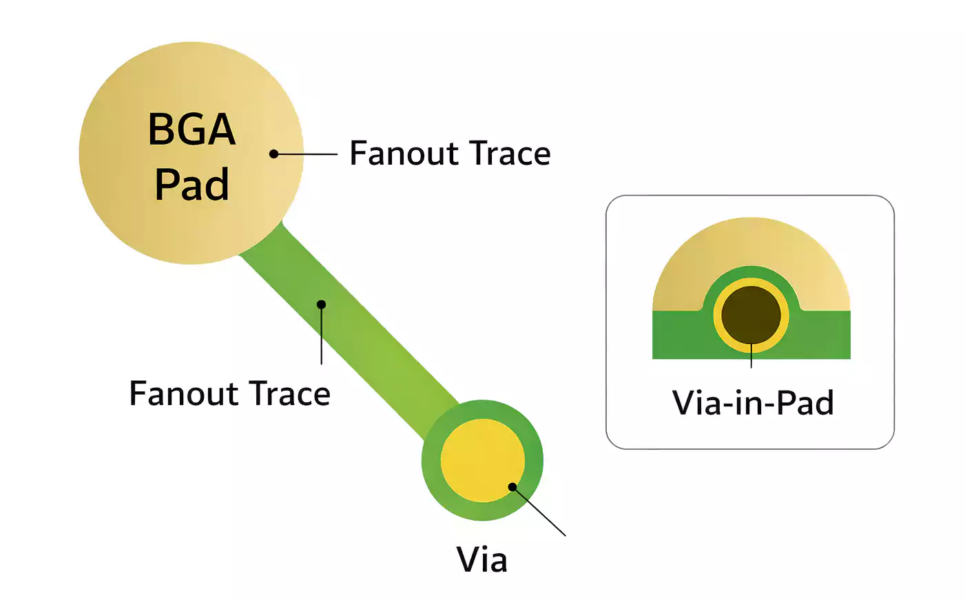
1. What Is BGA Fanout?
Fanout is the short escape connection from a BGA pad (ball) to a via or routing channel. It’s the transition from ultra-dense pad geometry to usable routing space.
In high-density designs, fanout determines:
- Whether signals can physically escape the package
- How many layers are required
- Whether HDI structures are necessary
- Whether routing congestion will occur later
If you don’t plan fanout first, you’ll likely end up:
- Adding unexpected layers
- Switching to blind/buried vias mid-design
- Fighting signal integrity issues.
- Increasing fabrication cost
2. Core Rule
Define your BGA fanout strategy before any global routing begins.
Treat the BGA as the center of gravity of the PCB. Memory, clocks, PMICs, and connectors should be arranged around it — not the other way around.
BGA Placement: Make Signals Short and Reliable
Placement decisions determine whether your layout is clean and efficient — or congested and fragile.
1. Central Positioning Strategy
For most processor-based designs, the main BGA should be placed near the center of the board. This helps:
- Distribute routing evenly in all directions.
- Improve thermal symmetry during reflow.
- Reduce mechanical stress concentration.
A centrally placed BGA typically results in a more balanced layout.
2. Keep Critical Devices Close
Place high-speed and timing-sensitive components as close to the BGA as possible:
- DDR memory – Minimize trace length and skew.
- Clock sources – Keep routing short and direct with minimal vias.
- PMICs – Short power loops improve power integrity.
- Flash devices – Reduce latency and impedance discontinuities.
Long signal paths increase:
- Skew mismatch
- Insertion loss
- Crosstalk
- Reflection risk
Shorter is almost always better.
3. Multi-BGA Systems
In designs with multiple large BGAs (CPU + FPGA, SoC + GPU), spacing becomes critical.
You must reserve routing channels between devices. Without them, the area between BGAs becomes a routing dead zone.
Plan this during floorplanning — not after routing begins.
4. How Close Can a BGA Be to the Board Edge?
A common question.
Recommended clearance: at least 7–10 mm from the BGA edge to the PCB edge.
Why?
- Board edges experience higher thermal gradients during reflow.
- Mechanical stress is amplified near edges.
- Uneven heating increases the risk of cold joints or solder defects.
Proper clearance improves assembly yield and long-term reliability.
Stack-Up Planning for BGA Breakout
Your stack-up often determines whether your BGA design is feasible.
1. Pitch Drives Technology
As the BGA pitch decreases:
- Pad-to-pad spacing shrinks
- Routing channels become narrower.
- Controlled impedance routing becomes harder.
- Standard through-hole vias may no longer fit.
Smaller pitch often requires:
- Thinner dielectrics
- Higher layer counts
- HDI stack-ups (1+N+1, 2+N+2)
- Microvias or via-in-pad
2. Estimating Required Layer Count
A practical rule of thumb:
- Roughly 60% of BGA balls are signals.
- The remaining balls are typically power and ground.
Power and ground balls can often drop directly to plane layers.
Signal balls require routing channels — and each layer can only escape a limited number of signals.
If inner rows cannot escape the surface layers, additional signal layers are required.
3. Continuous Reference Planes Are Mandatory
Every high-speed signal layer should have a solid adjacent reference plane.
Avoid:
- Routing over split ground planes
- Crossing plane voids
- Allowing return current paths to detour
Continuous reference planes ensure:
- Stable impedance
- Clean return paths
- Reduced EMI
- Strong signal integrity
BGA Fanout Strategy: Choosing the Right Breakout Method
Fanout isn’t one-size-fits-all. Your choice depends on pitch, cost, and fabrication capability.
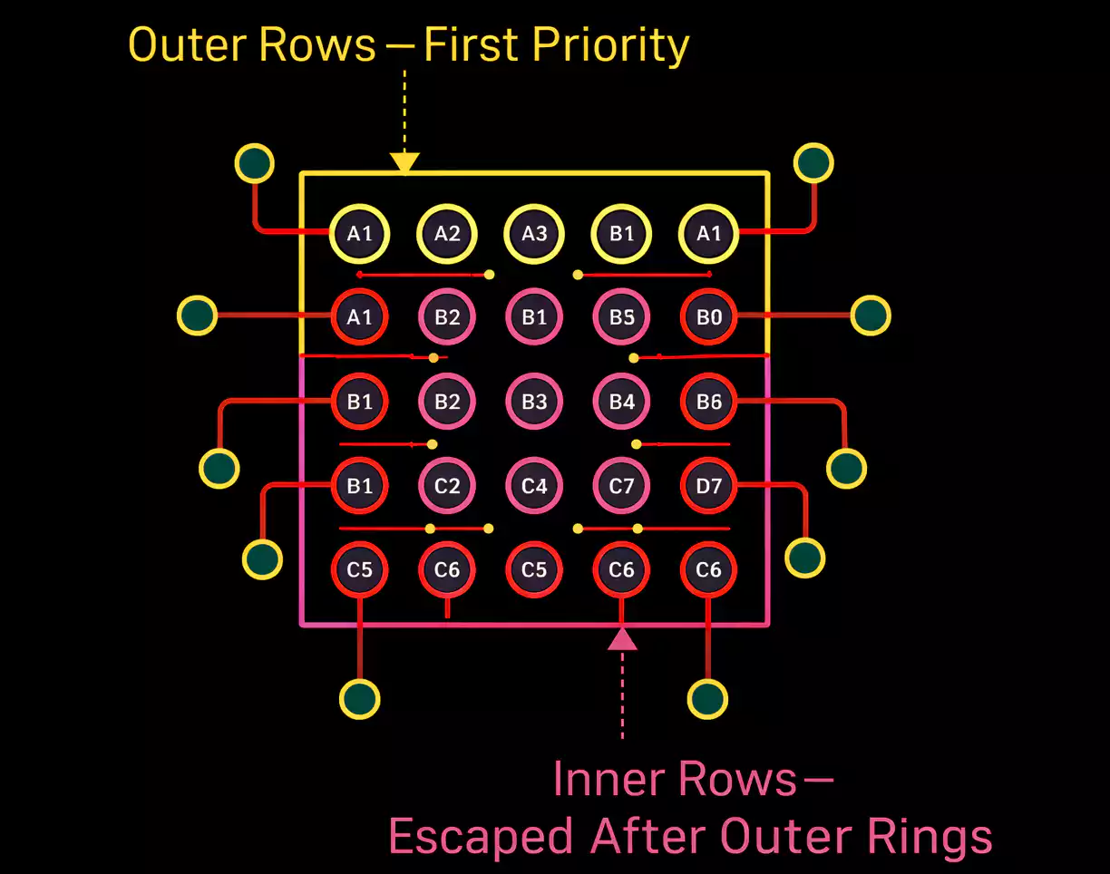
1. Outer Balls First (Outside-In Breakout)
Always route the outer one or two rows first.
Outer rows:
- Have more routing flexibility.
- Preserve channels for inner rows.
- Reduce congestion
If the outer routing space is wasted early, inner balls may become impossible to escape.
Fanout should proceed ring by ring, from the outside in.
2. Dog-Bone Fanout
The classic dog-bone structure consists of:
- A short trace (neck)
- A via (head)
Best suited for:
- Moderate pitch (e.g., 0.8 mm or larger)
- Standard through-hole processes
- Cost-sensitive designs
Dog-bone fanout is reliable, widely supported, and easy to manufacture.
3. Via-in-Pad (VIP)
When pitch shrinks to 0.5 mm or below, placing vias between pads may no longer be possible.
Via-in-pad places the via directly inside the pad and routes signals on inner layers.
Advantages:
- Maximum breakout density
- Clean routing channels
- Efficient use of space
Trade-offs:
- Requires filled and plated vias
- Higher fabrication cost
- Greater process control
Important: Use consistent breakout style across the entire BGA region. Mixing styles increases manufacturing risk.
Pad Design and Solder Mask Considerations
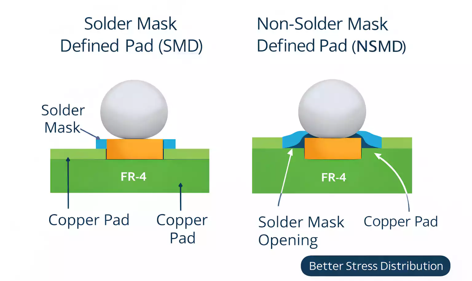
1. NSMD vs SMD Pads
In most BGA PCB board designs, NSMD (Non-Solder Mask Defined) pads are preferred.
Why NSMD?
- Full copper perimeter exposed.
- Better solder joint stress distribution
- Improved reliability
- Often, more routing flexibility
SMD pads may be used when tighter solder mask control or enhanced pad adhesion is required, but NSMD is generally the industry standard.
2. Solder Mask Bridge: The Hidden Risk
The solder mask bridge is the narrow strip of mask between adjacent pads.
It is the only physical barrier preventing solder bridging.
As pitch decreases:
- Mask bridges narrow
- Manufacturing tolerance becomes critical.
- Bridging risk increases
Always confirm your manufacturer’s minimum solder mask capability before finalizing pad geometry.
Via Rules and DFM Constraints
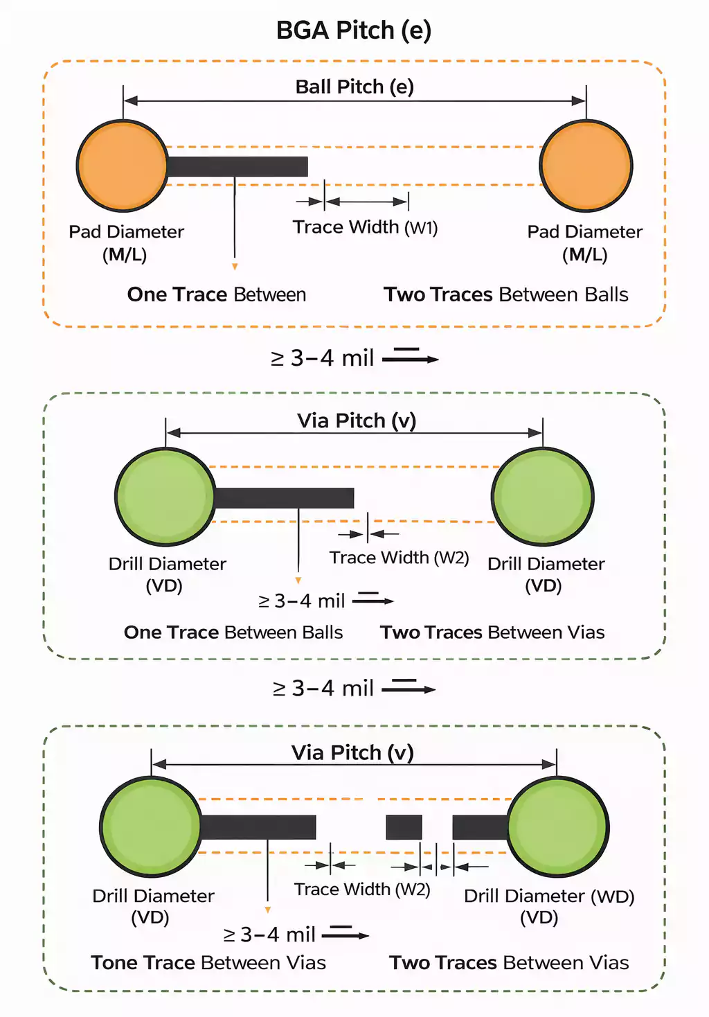
1. Minimum Via-to-Pad Spacing
Recommended minimum:
≥ 3–4 mil (0.075–0.1 mm) between via annular ring and pad edge.
If vias are too close:
- Solder mask bridges become fragile.
- Fabrication defects increase
- Solder reliability suffers
This rule alone prevents many BGA assembly failures.
2. Via-in-Pad Filling Requirements
If using via-in-pad:
- Vias must be properly filled (epoxy or copper)
- Surface must be planarized.
- Plating must be uniform.
Poor filling can cause solder wicking or voiding.
3. Design for Manufacturing Is Non-Negotiable
Verify early:
- Minimum line width/spacing
- Minimum drill size
- Annular ring requirements
- Mask alignment tolerance
Electrical design and manufacturing capability must align.
BGA Routing Best Practices
1. Orthogonal Routing Between Layers
Adjacent signal layers should be routed at 90° angles:
- Layer 1: Horizontal
- Layer 2: Vertical
- Layer 3: Horizontal
This reduces broadside crosstalk and improves routing clarity.
2. Limit Layer Transitions for High-Speed Signals
Every via introduces:
- Impedance discontinuity
- Stub effects
- Return path shifts
For signals above 1 GHz, aim to limit routing to one-layer transitions or fewer whenever possible.
Ideal path:
- Exit BGA pad
- Transition once
- Route directly to the destination
Fewer transitions mean better signal integrity.
3. Manage Via Stubs
Through-hole vias create unused stub lengths that act as resonant structures.
Mitigation options:
- Use microvias
- Backdrill unused sections
- Minimize via length
High-speed performance depends on controlling these parasitics.
Flip-Chip BGA: Additional Reliability Considerations
Flip-chip BGA packages introduce added mechanical and thermal sensitivity.
Key differences:
- Die is flipped and directly connected.
- The thermal path differs.
- Stress distribution changes
Design implications:
- Balanced layout symmetry
- Careful thermal via placement
- Controlled heat spreading
- Consistent land pattern geometry
Reliability becomes more dependent on mechanical balance and thermal management.
Final BGA PCB Board Checklist
Before releasing your design, confirm:
- Fanout is defined before routing.
- Outer balls are routed first.
- Continuous reference planes under high-speed nets
- NSMD pads are properly defined
- Via-to-pad spacing ≥ 3–4 mil
- BGA clearance ≥ 7–10 mm from board edge
- High-speed nets are limited to minimal layer transitions.
- Orthogonal routing between adjacent signal layers
If these conditions are met, your BGA PCB board is far more likely to pass fabrication and assembly without surprises.
Conclusion
BGA PCB board design is a disciplined engineering process. It’s not just about density — it’s about balance:
- Placement that minimizes the critical path length
- Fanout that preserves routing flexibility
- Stack-up that supports clean return paths
- Pad and via rules aligned with manufacturing capability
- Routing that protects signal integrity
When these elements are addressed systematically, you achieve high performance, manufacturability, and long-term reliability.
At FastTurnPCB, we work closely with engineering teams to ensure BGA layouts are optimized for both performance and production. Whether your project requires standard multilayer boards or advanced HDI BGA technology, aligning layout strategy with fabrication capability is the key to first-pass success.