

Introduction
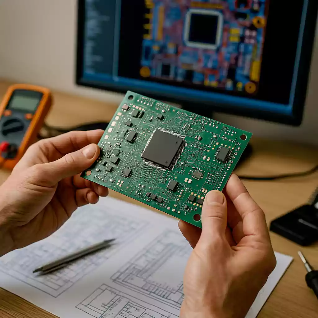
A Printed Circuit Board (PCB) is a flat, layered board used to mechanically support and electrically connect electronic components. It serves as the backbone of virtually all modern electronic devices—from smartphones and laptops to medical equipment and industrial machinery.
Made from insulating material and laminated with copper traces, a PCB allows signals and power to travel efficiently between components without the need for bulky wiring. Its design enables compact, reliable, and high-speed electronics that define today's digital world.
This article provides a clear and comprehensive overview of what a PCB is, how it works, the different types available, and its critical role in the design and manufacturing of electronic systems. Whether you're curious about how electronics function or looking to deepen your technical understanding, this guide covers everything you need to know about PCBs.
What Is a PCB?
A Printed Circuit Board (PCB) is a flat board made of non-conductive material that supports and connects electronic components using conductive tracks, pads, and other features etched from one or more layers of copper. PCBs are essential to virtually all electronic circuits, providing a compact, organized, and efficient way to interconnect components like resistors, capacitors, microchips, and connectors.
Full Form of PCB and Its Function
The term PCB stands for Printed Circuit Board. Its primary function is twofold:
- Mechanical Support – PCBs provide a stable physical platform to mount electronic components.
- Electrical Connectivity – They facilitate the flow of electricity through carefully designed copper traces, replacing traditional point-to-point wiring.
This allows modern electronics to be smaller, more reliable, and easier to mass-produce.
Why PCBs Are Essential in Electronics
Before PCBs, circuits were built using hand-soldered wires and point-to-point connections, which were bulky, error-prone, and hard to maintain. The invention of PCBs revolutionized electronics by offering:
- Compact design – Components are neatly arranged on a single board.
- Improved reliability – Reduced chances of loose connections or short circuits.
- Mass production capability – PCBs can be fabricated in large quantities with consistent quality.
- Ease of maintenance – Identifiable layout makes troubleshooting and repair simpler.
Common Materials Used in PCBs
The base of a PCB is typically made from fiberglass-reinforced epoxy laminate (FR-4), which provides structural strength and electrical insulation. Copper is laminated onto the board's surface and then etched to form pathways for electric signals.
In specialized applications, materials like ceramic, Teflon, or flexible polyimide may be used to achieve specific electrical or mechanical performance.
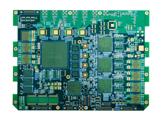
PCB Structure and Types
Printed Circuit Boards come in a variety of forms, depending on the complexity and performance requirements of the electronic system. The internal structure of a PCB and its classification—single-layer, double-layer, or multi-layer—directly impact its function, cost, and manufacturing process.
Below is a comparison of the most common types of PCBs:
| PCB Type | Number of Layers | Structure | Common Applications | Key Advantages |
|---|---|---|---|---|
| Single-Sided PCB | 1 | One layer of copper on one side of the base material. | Low-cost electronics, LED lighting, toys | Simple, low-cost, easy to produce |
| Double-Sided PCB | 2 | Copper layers on both sides with plated through-holes (vias) connecting them. | Power supplies, HVAC systems, automotive electronics | Increased routing space, more design flexibility |
| Multi-Layer PCB | 3 or more | Multiple copper layers sandwiched between insulating layers. | Smartphones, servers, medical devices, aerospace | Compact size, high performance, suitable for HDI needs |
| Rigid PCB | Varies | Made with solid fiberglass (typically FR-4). | Computers, TVs, industrial control systems | Durable, stable, cost-effective |
| Flexible PCB | Varies | Built on flexible plastic substrate like polyimide. | Wearables, cameras, mobile devices | Lightweight, bendable, space-saving |
| Rigid-Flex PCB | Varies | Combines rigid and flexible sections in one board. | Medical implants, military equipment, foldable tech | Compact, durable, optimized for dynamic use |
| HDI PCB | Multi-layer | High-Density Interconnect with microvias, fine lines, and thin materials. | Smartphones, tablets, high-speed devices | High signal integrity, dense component integration |
| Metal Core PCB | Usually single/double | Includes a metal (usually aluminum) base for heat dissipation. | LED systems, power electronics | Excellent thermal management |
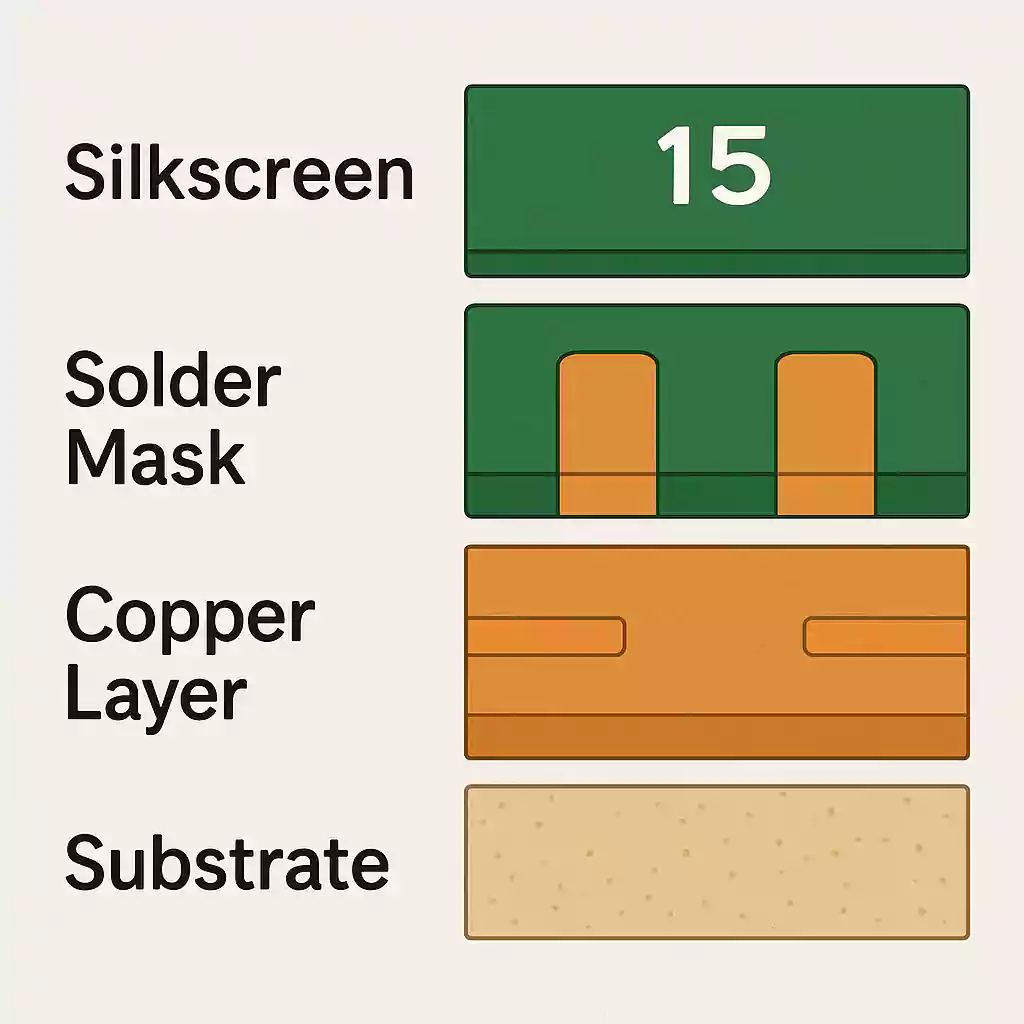
Key Structural Elements of a PCB
Regardless of type, most PCBs are built from the following core layers:
- Substrate (Base Material) – Usually FR-4, providing mechanical support.
- Copper Layer – Conductive layer for signal and power transmission.
- Solder Mask – Protective layer that insulates copper traces and prevents short circuits.
- Silkscreen – Printed markings for labels, symbols, and component references.
PCB Manufacturing and Design Process Explained
The process of creating a printed circuit board (PCB) involves both designing the layout and manufacturing the physical board. This section breaks down each step to help you understand how an idea becomes a functioning electronic circuit.
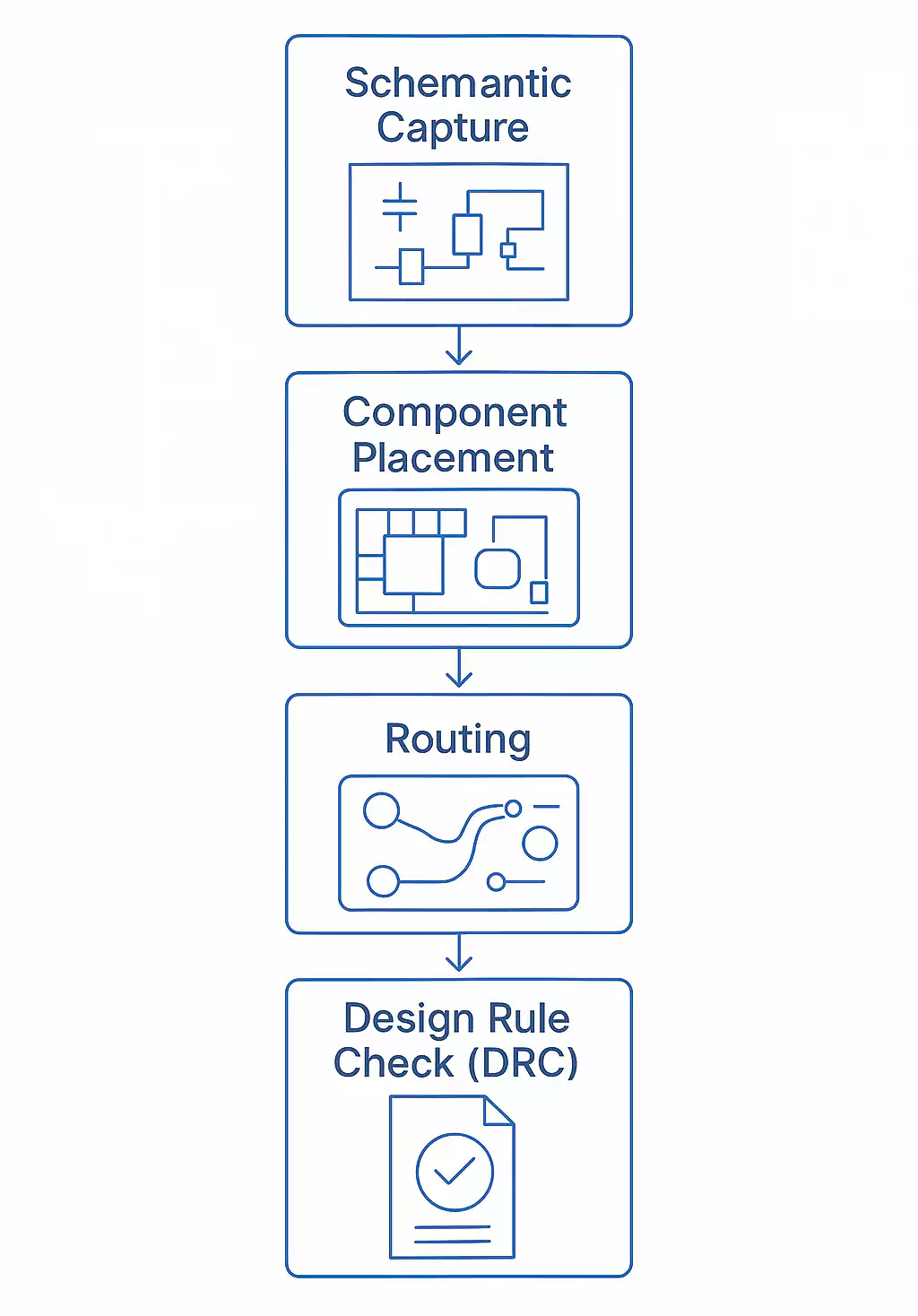
1. PCB Design Phase
The design process begins with the use of Electronic Design Automation (EDA) or CAD software such as Altium Designer, KiCad, or Eagle. The goal is to translate a circuit schematic into a functional layout.
Key steps in PCB design include:
- Schematic Capture
Define the electrical connections between components in a circuit diagram. - Component Placement
Arrange components logically and efficiently on the board to optimize space and signal flow. - Routing
Create copper traces that connect pins and components based on the schematic. This involves single-layer, double-layer, or multi-layer routing depending on complexity. - Design Rule Check (DRC)
Software validation to ensure there are no errors, such as overlapping traces or insufficient spacing. - Gerber File Generation
The final output is a set of manufacturing files (Gerber, NC Drill, BOM) sent to PCB fabrication houses.
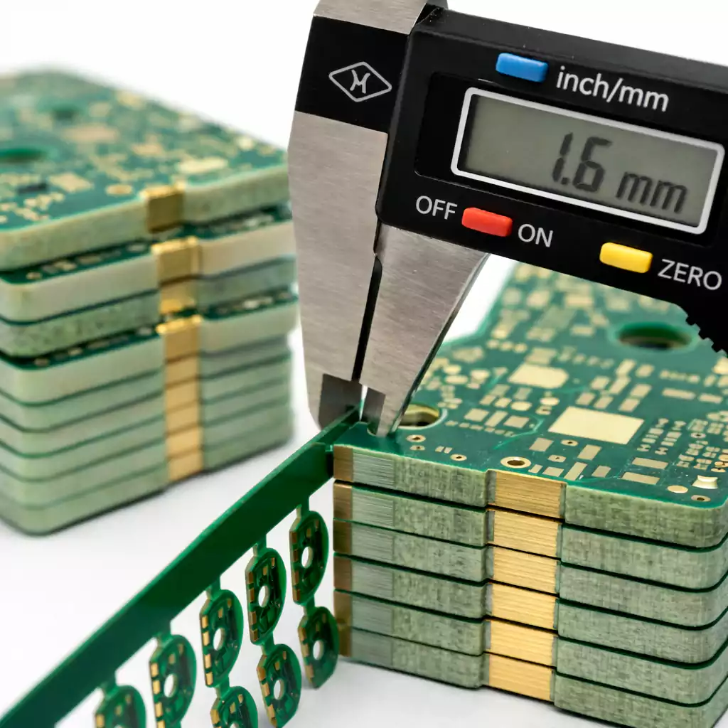
2. PCB Fabrication Process
Once the design is finalized, the PCB is manufactured using a series of precise industrial steps:
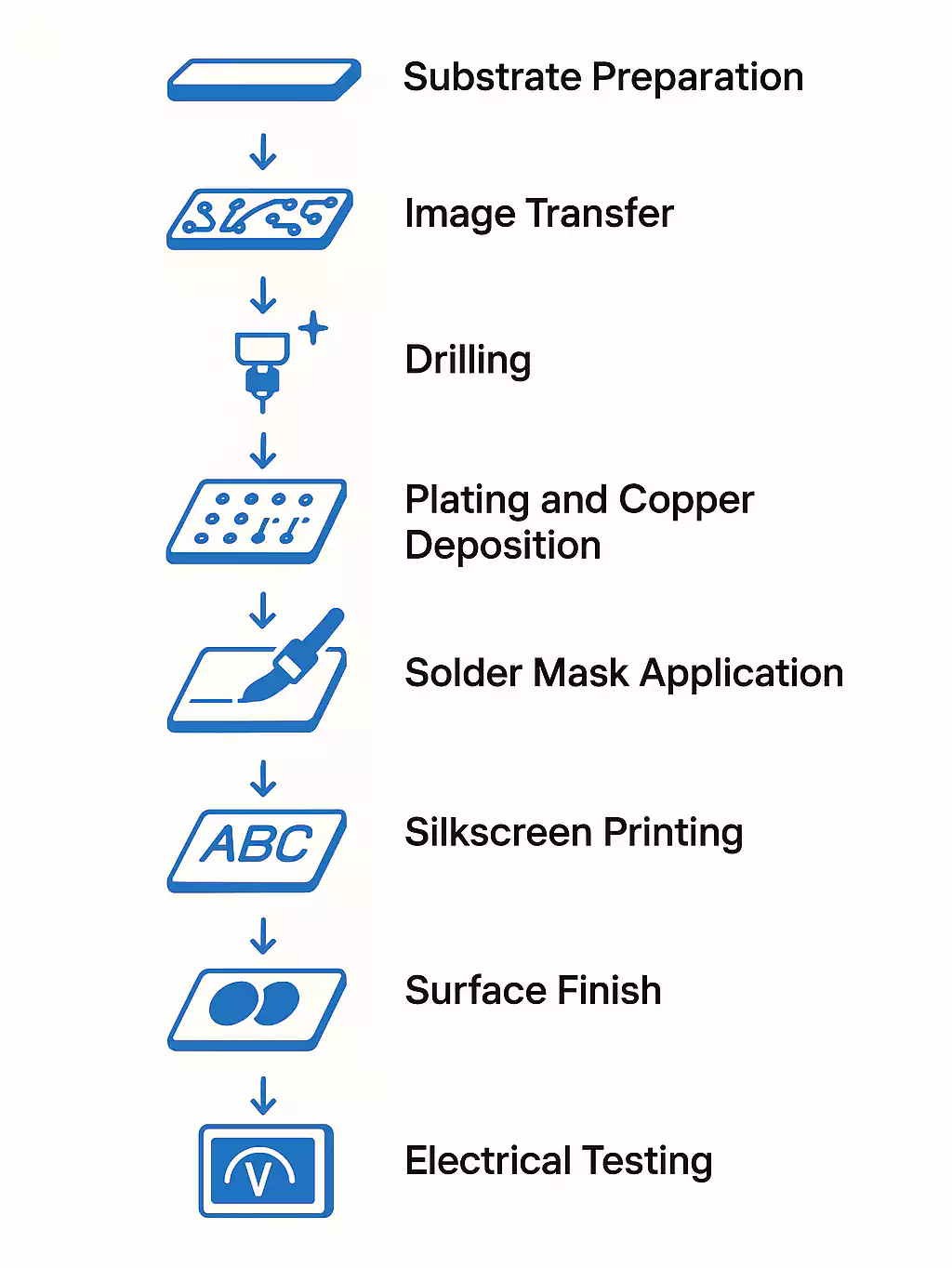
Step-by-step PCB manufacturing process:
- Substrate Preparation
Start with a base material like FR-4 or polyimide, laminated with copper foil. - Image Transfer (Photoresist & UV Exposure)
The circuit pattern is transferred onto the copper using photoresist and UV light exposure. - Etching
Unwanted copper is removed using chemical etching, leaving only the desired copper traces. - Drilling
Precision holes (vias) are drilled to connect different layers or mount components. - Plating and Copper Deposition
Copper is electroplated inside the drilled holes to establish electrical continuity. - Solder Mask Application
A protective solder mask is applied to prevent short circuits and oxidation. - Silkscreen Printing
Identifiers like labels, logos, and component outlines are printed using silkscreen. - Surface Finish
Apply finishes like HASL, ENIG, or OSP to enhance solderability and prevent corrosion. - Electrical Testing
Every PCB is tested for short circuits and open circuits to ensure functionality.
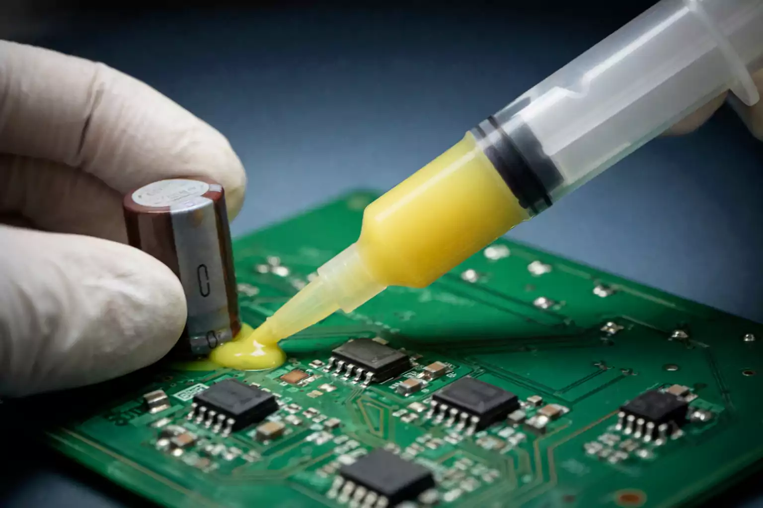
3. PCB Assembly (PCBA)
After fabrication, the PCB undergoes assembly, where electronic components are soldered onto the board.
Two main assembly techniques:
- Through-Hole Technology (THT) – Components with leads inserted into drilled holes.
- Surface Mount Technology (SMT) – Components are placed directly on the board surface and soldered, often by automated machines.
High-volume production typically uses automated pick-and-place machines, reflow ovens, and wave soldering systems.
4. Quality Control and Testing
To ensure reliability and performance, manufacturers perform various inspections:
- Automated Optical Inspection (AOI)
- X-ray Inspection (for BGA and multilayer defects)
- In-Circuit Testing (ICT)
- Functional Testing to simulate real-world performance
Applications and Market Trends of PCBs
Widespread Applications of PCBs
Printed Circuit Boards (PCBs) are used in nearly every electronic product across a wide range of industries:
- Consumer Electronics: Smartphones, tablets, laptops, televisions, and wearables all rely on compact, multi-layer PCBs to manage high-speed signals and power distribution.
- Automotive Industry: Modern vehicles use PCBs for engine control units (ECUs), infotainment systems, sensors, battery management in EVs, and advanced driver-assistance systems (ADAS).
- Medical Devices: PCBs are integral to medical equipment like MRI scanners, pacemakers, glucose monitors, and portable diagnostic tools, where reliability and miniaturization are critical.
- Industrial Equipment: Automation systems, robotics, power supplies, and control panels all utilize durable, high-performance PCBs.
- Aerospace and Defense: PCBs in these sectors must meet extreme reliability standards for use in radar systems, navigation equipment, satellite communications, and avionics.
Global Market Trends and Growth
The global PCB market continues to grow, driven by rapid advancements in electronics, 5G infrastructure, electric vehicles, and IoT devices.
- As of 2024, the global PCB market is valued at approximately $80.3 billion, with projections to surpass $96.5 billion by 2029, growing at a CAGR of 3.8%.
- High-Density Interconnect (HDI) PCBs, flexible PCBs, and metal core PCBs are among the fastest-growing segments due to increasing demand for smaller, lighter, and heat-efficient designs.
- Asia-Pacific remains the largest manufacturing hub, especially China, Taiwan, South Korea, and Japan, while North America and Europe focus on high-end, specialized PCBs for automotive and defense.
Emerging Technology Trends
- Flexible and Rigid-Flex PCBs are gaining popularity in wearable tech and foldable devices.
- 3D printed PCBs and embedded components are shaping next-gen electronics with compact, custom layouts.
- Sustainable PCB materials and green manufacturing practices are also emerging as environmental regulations tighten.
Frequently Asked Questions (FAQ)
What is the difference between PCB and PCBA?
A PCB (Printed Circuit Board) is the bare board with copper traces and no components mounted. A PCBA (Printed Circuit Board Assembly) refers to the PCB after components have been soldered onto it. In short, PCBA = PCB + components.
What does a via do on a PCB?
A via is a small hole that allows electrical connections between different layers of a PCB. There are several types: through-hole vias, blind vias, and buried vias, each used based on the board’s layer structure and signal routing needs.
What materials are commonly used in PCB manufacturing?
The most common base material is FR-4, a fiberglass-reinforced epoxy laminate. For specific needs, polyimide, ceramic, or metal core materials may be used. Copper is typically used for the conductive layers.
What is the purpose of a solder mask?
A solder mask is a protective layer that covers the copper traces on a PCB. It prevents oxidation, reduces the risk of short circuits, and ensures that solder only sticks to exposed pads during assembly.
What’s the difference between single-layer and multi-layer PCBs?
•Single-layer PCBs have one copper layer and are used in simple, low-cost electronics.
•Multi-layer PCBs have three or more layers of copper, enabling more complex, high-density circuit designs.
What surface finishes are used on PCBs?
Common PCB surface finishes include:
•HASL (Hot Air Solder Leveling)
•ENIG (Electroless Nickel Immersion Gold)
•OSP (Organic Solderability Preservative)
Each affects solderability, shelf life, and cost.
How do I choose the right type of PCB?
It depends on the application:
•Rigid PCBs for durable, stable environments.
•Flexible PCBs for wearables or curved devices.
•Metal core PCBs for heat-sensitive applications like LEDs.
•HDI PCBs for high-speed, compact devices like smartphones.
What are common PCB design mistakes to avoid?
Some of the most frequent errors include:
•Inadequate trace width for current
•Poor via placement
•Overcrowded components
•Ignoring thermal management
•Skipping design rule checks (DRC)
Misconceptions
Common Misconceptions About PCBs
1. More Layers Always Mean Better Performance
While multi-layer PCBs can support more complex and high-speed circuits, they are not always necessary. For simple or low-power applications, single- or double-layer PCBs are more cost-effective and easier to manufacture. Adding more layers unnecessarily increases production costs and design complexity.
2. All PCB Materials Perform the Same
Not all PCBs are created equal. Standard FR-4 works for most general-purpose electronics, but high-frequency or high-temperature applications require specialized materials like Rogers, polyimide, or aluminum-based cores. Using the wrong material can lead to signal loss or heat damage.
3. Thicker Copper = Better in All Cases
While thicker copper improves current-carrying capacity and durability, it also increases cost and can complicate trace routing. For high-frequency signals, thicker copper can even introduce unwanted parasitics. Copper thickness should match the application's electrical and thermal demands.
4. Designing for Appearance is More Important Than Function
A neat-looking PCB layout doesn't guarantee performance. Signal integrity, impedance control, thermal flow, and grounding are far more critical than aesthetics. Function should always drive form in PCB design.
Conclusion
Printed Circuit Boards (PCBs) are the fundamental building blocks of nearly all modern electronics. From simple household gadgets to advanced aerospace systems, PCBs provide the electrical connectivity, structural support, and signal integrity required for reliable performance.
In this guide, we've covered:
- What a PCB is and why it's essential
- Common PCB types and structural components
- The design and manufacturing process
- Real-world applications and industry trends
- Frequently asked questions and common misconceptions
- Key performance factors like thermal management and signal integrity
Understanding how PCBs work—and how they are designed and manufactured—empowers you to make better decisions whether you're an engineer, product developer, student, or electronics enthusiast.