


Introduction
Whether you're developing a compact consumer device,a robust industrial controller,or a high-frequency communication system,PCB thickness plays a critical role in mechanical strength,signal performance,thermal behavior,and overall manufacturing cost.
The standard PCB thickness most commonly referenced across the electronics industry is 1.57 mm (0.062 inches). This value has become a de facto benchmark due to its long-standing compatibility with through-hole components and manufacturing processes. However, in practice, PCB thickness can range from 0.2 mm to over 3.2 mm, depending on factors such as layer count, copper weight, dielectric material, and specific application requirements.
This article goes beyond simply listing dimensions. It addresses why PCB thickness matters, what influences it, and how to choose the right thickness based on real-world scenarios. You'll also learn how manufacturing constraints, electrical performance, and mechanical considerations come together to define the optimal board thickness for your project.
Whether you're a hardware startup founder, a PCB design engineer, or just curious about board specifications, this guide will equip you with all the insights needed to make informed, cost-effective, and technically sound decisions.
PCB Thickness Fundamentals: What It Is and How It's Measured
Before diving into how to choose the right PCB thickness, it's essential to understand what this measurement actually represents and how it impacts PCB performance and manufacturability.
What Does PCB Thickness Mean?
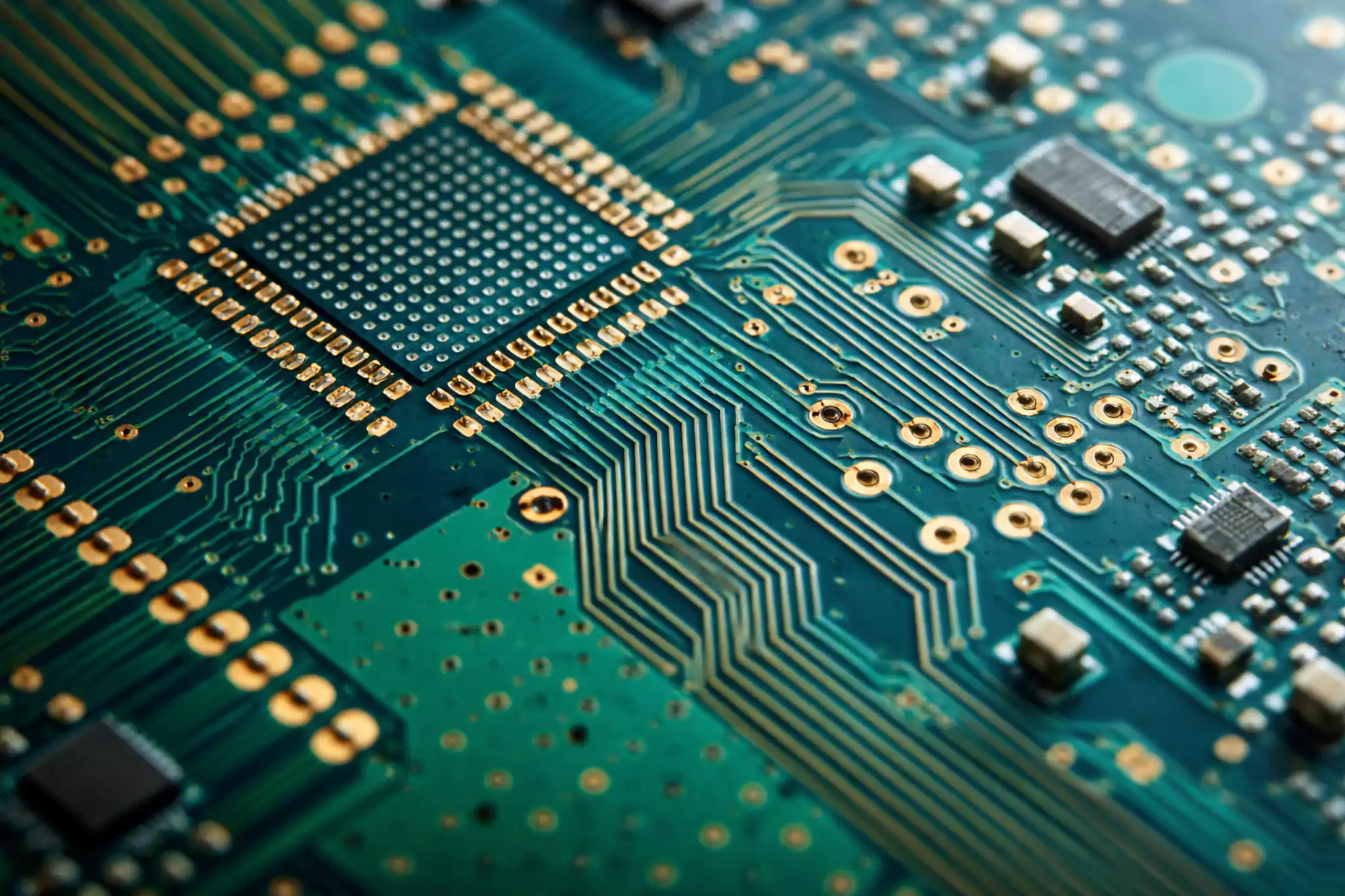
PCB thickness refers to the total vertical height of the finished printed circuit board, including all its constituent layers: copper foil, core substrate, prepreg (pre-impregnated resin), and any surface finishes. It is typically measured in either millimeters (mm) or inches (in), with the standard measurement being 1.57 mm (0.062 inches)—a value rooted in legacy material dimensions used in early PCB manufacturing.
Quick Conversion Reference:
- 1.57 mm = 0.062 inches
- 0.8 mm = 0.031 inches
- 2.36 mm = 0.093 inches
- 3.2 mm = 0.125 inches
Breakdown of a PCB's Structure
A PCB isn't just a flat sheet—it's a multilayered structure composed of:
- Copper Layers: These are the conductive paths that carry electrical signals and power. Thicker copper layers (measured in ounces per square foot, such as 1 oz or 2 oz) can significantly impact overall board thickness.
- Core Material (Typically FR-4): A rigid fiberglass-reinforced epoxy laminate that gives the PCB mechanical strength and electrical insulation.
- Prepreg: A resin-impregnated fiberglass material placed between layers to bond them together during lamination. It adds to the board thickness and affects dielectric spacing.
- Soldermask and Surface Finish: While usually thin, these outermost coatings still contribute marginally to total thickness.
Why 1.57 mm Became the "Standard" Thickness
The origin of the 1.57 mm (0.062-inch) standard dates back to the plywood industry, where this was a common panel thickness. When early PCB manufacturers adopted similar equipment and tooling, this dimension was inherited as a norm. Over time, this became the industry standard due to compatibility with traditional through-hole components, connector slots, and chassis mounting requirements.
Modern Tolerances and Variability
While 1.57 mm remains a popular default, today's boards come in a wide variety of thicknesses based on specific needs. PCB manufacturers typically offer custom thickness options with tolerances as tight as ±10%, depending on materials, layer count, and copper weight.
By understanding what PCB thickness truly involves—from its composition to its historical context—you'll be better prepared to evaluate your project requirements and engage effectively with manufacturers. In the next section, we'll explore the standard thickness options available today and how they align with industry use cases.
Standard PCB Thickness Values & Manufacturer Ranges
While 1.57 mm (0.062 inches) is the most widely recognized standard PCB thickness, today's manufacturing capabilities support a wide range of board thicknesses to meet the needs of different applications. Choosing the right thickness depends on factors such as mechanical constraints, component compatibility, current-carrying requirements, and signal performance.
Below is a comparison table that outlines common PCB thickness options, their typical applications, and manufacturer availability:
| PCB Thickness | Inches | Common Use Cases | Layer Count | Manufacturer Availability |
|---|---|---|---|---|
| 0.2 mm | 0.0079 in | Ultra-thin PCBs, flexible circuits, wearables | 1–2 layers | Limited (custom order only) |
| 0.4 mm | 0.0157 in | Compact consumer electronics, mobile devices | 2–4 layers | Widely available |
| 0.6 mm | 0.0236 in | Space-constrained products, RF modules | 2–6 layers | Common |
| 0.8 mm | 0.0315 in | LED boards, handheld devices | 2–6 layers | Very common |
| 1.0 mm | 0.0394 in | Moderate-density PCBs, low-profile connectors | 4–8 layers | Common |
| 1.2 mm | 0.0472 in | High-speed digital circuits, denser boards | 6–10 layers | Common |
| 1.57 mm (Standard) | 0.062 in | General-purpose PCBs, through-hole components | 2–10+ layers | Industry standard |
| 2.0 mm | 0.0787 in | Ruggedized industrial applications, automotive | 6–12+ layers | Available from most vendors |
| 2.4 mm | 0.0945 in | High-current PCBs, power electronics | 8–12+ layers | Less common, higher cost |
| 3.2 mm | 0.125 in | Heavy-duty applications, large format PCBs | 10–16+ layers | Special order / niche use |
🛠️ Tip: Most manufacturers offer a default range between 0.8 mm and 1.6 mm, with custom thicknesses available upon request. Always verify availability and minimum order quantities with your PCB supplier.
Key Takeaways
- Standard ≠ One-size-fits-all: While 1.57 mm is a default, many applications benefit from thinner or thicker PCBs.
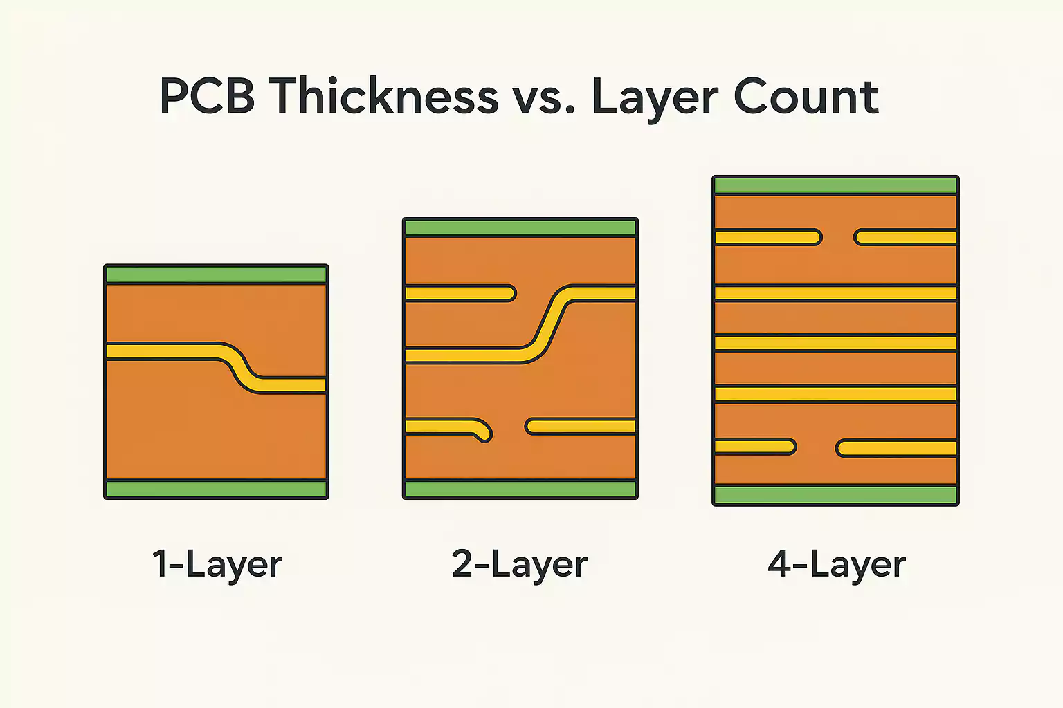
- Layer Count Impacts Thickness: More layers typically require thicker boards to accommodate insulation and copper distribution.
- Customization Is Possible: Leading manufacturers like JLCPCB, PCBWay, and Advanced Circuits offer configurable thickness options with precise tolerances.
- Design Around Available Specs: For cost-efficiency and faster turnaround, select from your manufacturer's standard stack-up offerings whenever possible.
Key Factors That Influence PCB Thickness Selection
Choosing the optimal PCB thickness isn't just about matching industry standards — it's a strategic decision that balances electrical performance, mechanical strength, manufacturability, and cost. Below are the most critical factors that influence how thick your PCB should be:
1. Number of Layers (Layer Stack-Up)
The number of copper layers directly affects board thickness.
- Single- and double-sided PCBs can stay under 1.0 mm due to minimal stack-up.
- Multilayer boards (4–16+ layers) require additional dielectric and prepreg layers, naturally increasing thickness.
- More layers = more insulation, routing complexity, and height.
Tip: Standard 4-layer boards typically fall between 1.0 mm and 1.6 mm, while 8+ layer boards may exceed 2.0 mm.
2. Copper Thickness
Copper thickness — often expressed in ounces (oz) per square foot — has a significant impact on total board height.
- Common values: 1 oz (35 μm), 2 oz (70 μm), and heavy copper (up to 6 oz+).
- Thicker copper allows for higher current-carrying capacity but increases both overall PCB thickness and manufacturing cost.
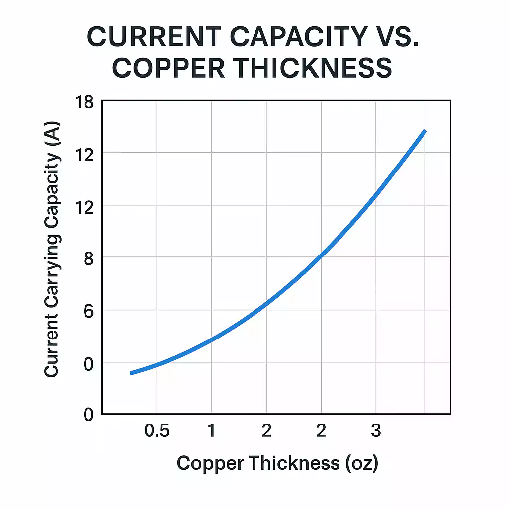
Use heavy copper in power supply boards or motor controllers; stick to 1 oz for signal layers in digital designs.
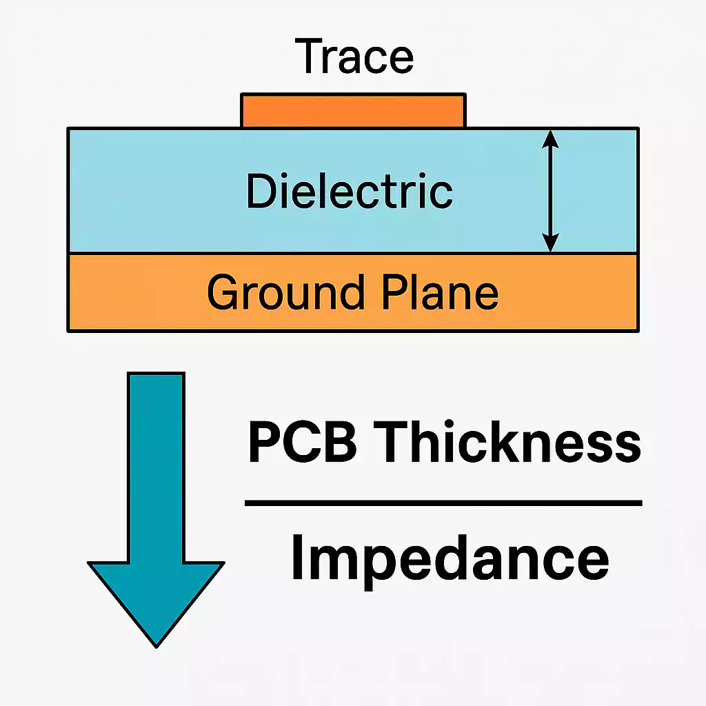
3. Signal Integrity & Impedance Control
For high-speed digital and RF designs, the controlled impedance of traces is vital.
- Impedance depends on the trace width, copper thickness, and the distance between signal layers and reference planes, which is affected by board thickness.
- A thicker board may introduce higher inductance and signal loss over long traces if not properly designed.
Use case: If designing a USB 3.0 or HDMI interface, the PCB stack-up and dielectric spacing must meet tight impedance specs, affecting thickness.
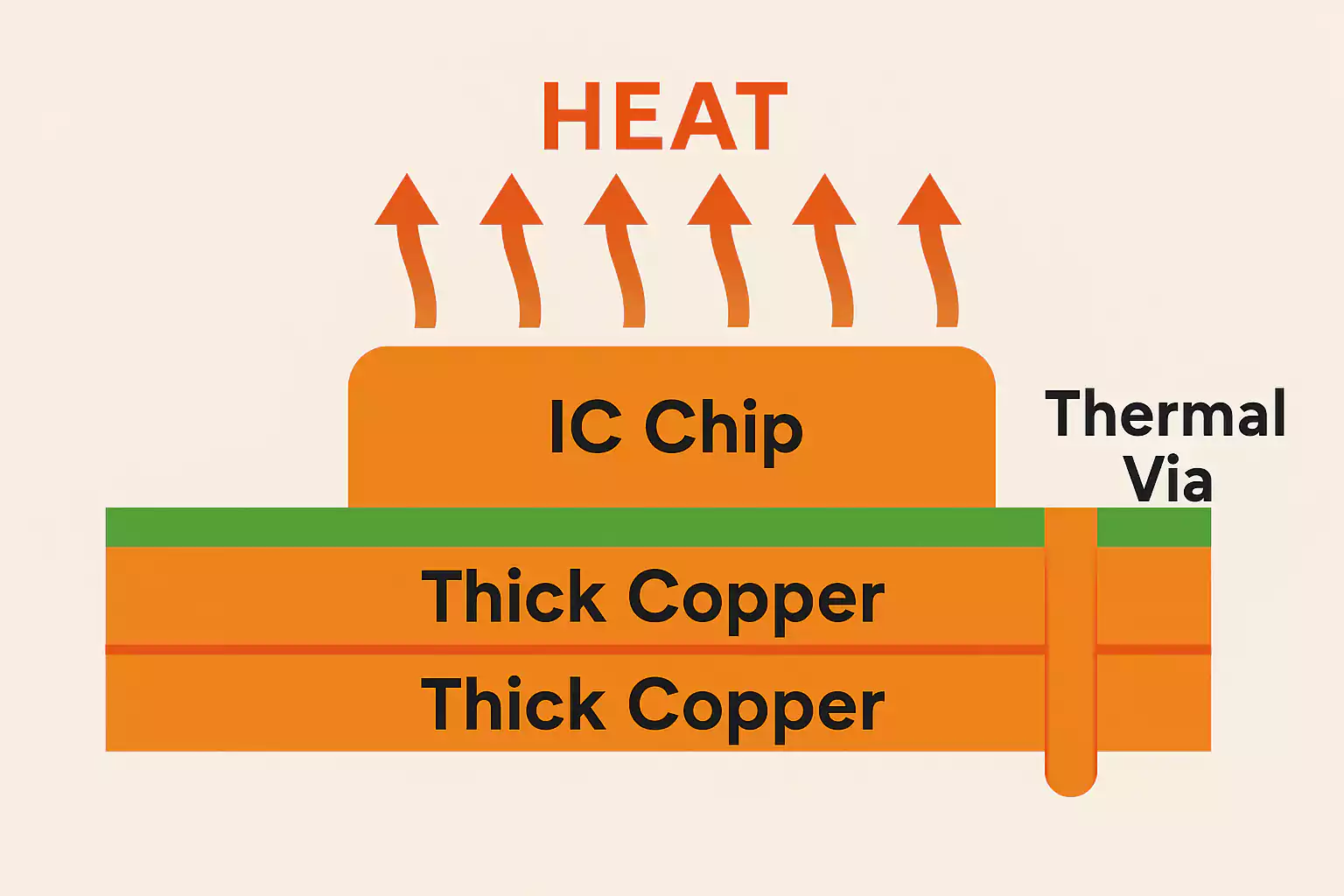
4. Thermal Performance and Heat Dissipation
Thicker PCBs with more copper or thermal vias can dissipate heat more efficiently, reducing thermal stress on components.
- Applications like LED lighting, power amplifiers, and battery management systems often demand thicker boards for thermal reliability.
Heat-generating devices benefit from 2.0 mm+ PCBs with thermal pads or heat sinks integrated into the stack-up.
5. Mechanical Strength and Flexural Rigidity
Mechanical durability is critical for boards exposed to vibration, insertion/removal forces, or bending.
- Thicker PCBs provide higher stiffness, making them ideal for automotive, industrial, or connector-heavy applications.
- Conversely, thinner PCBs (≤0.6 mm) are preferred in flexible or curved enclosures, such as in wearable electronics.
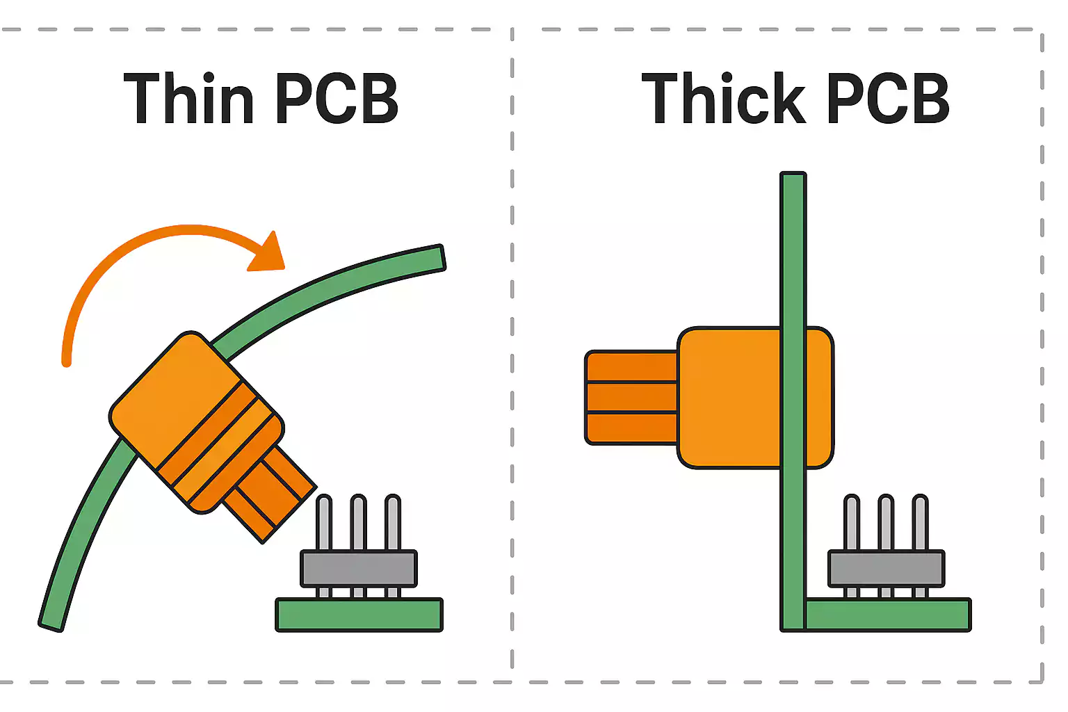
PCB thickness can also affect connector alignment and enclosure fit, so always check tolerances.
6. Manufacturing Capabilities and Cost
Not all PCB fabs support ultra-thin or ultra-thick boards.
- Standard thicknesses (0.8–1.6 mm) are more economical and have shorter lead times.
- Custom thicknesses may increase tooling time, cost, or minimum order quantity.
Pro tip: Always consult your PCB manufacturer's stack-up guide to avoid unmanufacturable designs.
Summary Table: Thickness Considerations by Factor
| Factor | Thin PCB (<1.0 mm) | Thick PCB (>1.6 mm) |
|---|---|---|
| Layer count | 1–2 layers | 6+ layers |
| Copper weight | 0.5–1 oz | 2–6+ oz |
| Signal performance | Moderate-speed circuits | High-speed or high-isolation needs |
| Thermal dissipation | Minimal heat loads | High-current, thermally demanding environments |
| Mechanical use | Compact, lightweight designs | Rugged, high-force or load-bearing designs |
| Cost & availability | Cheaper, widely available | Higher cost, may require custom quote |
By taking these factors into account early in your design process, you can avoid common pitfalls, ensure performance, and streamline manufacturing. In the next section, we'll dive deeper into real-world application scenarios and how thickness varies across industries like consumer electronics, automotive, and telecommunications.
Application-Specific Recommendations for Choosing PCB Thickness
While standard PCB thickness (such as 1.57 mm) is a reliable starting point, optimal thickness often depends on your product's form factor, environmental conditions, signal requirements, and mechanical constraints. Below are best practices and recommendations for selecting PCB thickness across various industry applications.
1. Consumer Electronics (Phones, Tablets, Wearables)
- Recommended Thickness: 0.4 mm – 1.0 mm
- Why: These products prioritize slim profiles and light weight. Thinner boards allow compact device assembly but still must maintain structural integrity.
- Notes: Consider using flex or rigid-flex PCBs where bending is required. Use 0.8 mm for mid-range strength and compatibility with SMT.
2. Industrial Equipment & Power Electronics
- Recommended Thickness: 1.6 mm – 2.4 mm+
- Why: These systems often require high current handling, mechanical robustness, and thermal dissipation. Thicker copper and multi-layer boards are common.
- Notes: Use 2 oz or heavier copper layers and thermal vias to improve performance. 2.0 mm or more is typical in motor controllers or power converters.
3. Automotive Applications
- Recommended Thickness: 1.6 mm – 2.0 mm
- Why: Automotive PCBs endure temperature extremes, vibration, and mechanical shock. Moderate thickness with high reliability is preferred.
- Notes: Use high Tg materials, heavy copper layers, and conformal coatings. Balance between rigidity and thermal conductivity is critical.
4. High-Frequency and RF Applications
- Recommended Thickness: 0.8 mm – 1.6 mm
- Why: These boards require precise impedance control. Thinner boards help reduce dielectric height, improving signal performance.
- Notes: Match dielectric thickness to controlled impedance targets (e.g., 50Ω). Materials like Rogers or PTFE substrates may be used.
5. LED Lighting Modules
- Recommended Thickness: 1.0 mm – 1.6 mm
- Why: LED boards must dissipate heat efficiently while remaining structurally stable. Aluminum-backed PCBs (MCPCBs) often use this thickness range.
- Notes: Use thick copper layers and thermal interface materials for maximum heat conduction.
SEO Keywords: MCPCB thickness for LED, aluminum PCB for lighting
6. Medical Devices
- Recommended Thickness: 0.6 mm – 1.2 mm
- Why: Many medical PCBs are used in compact or portable diagnostic tools that require precision and reliability.
- Notes: Must comply with IPC Class III standards. Use high-reliability materials and avoid excessive thickness unless needed for durability.
7. Networking and Data Communication Hardware
- Recommended Thickness: 1.0 mm – 1.6 mm
- Why: Routers, switches, and server boards handle high-speed differential signals. Balanced thickness is essential for impedance control and heat management.
- Notes: Use 4 to 12 layers and ensure controlled stack-up designs for signal integrity.
Summary Table: PCB Thickness by Application
| Application | Recommended Thickness | Key Considerations |
|---|---|---|
| Consumer Electronics | 0.4 – 1.0 mm | Thin profile, lightweight, some flexibility |
| Industrial Power | 1.6 – 2.4 mm+ | Current capacity, heat, mechanical durability |
| Automotive | 1.6 – 2.0 mm | Vibration resistance, temperature stability |
| RF / High-Frequency | 0.8 – 1.6 mm | Impedance control, low dielectric spacing |
| LED Lighting | 1.0 – 1.6 mm | Thermal conductivity, aluminum base options |
| Medical Devices | 0.6 – 1.2 mm | Reliability, space-saving design |
| Networking Equipment | 1.0 – 1.6 mm | High-speed routing, signal integrity |
By tailoring PCB thickness to your application, you can optimize for performance, reliability, and cost. In the next section, we'll dive into layer stack-up design strategies, including how to control dielectric thickness and work with manufacturers to build your ideal board.
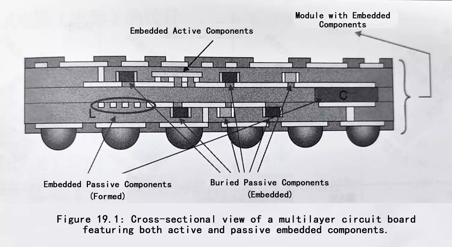
Practical Stack-Up Design Guide: Building the Right PCB Thickness from the Inside Out
Choosing a PCB thickness isn't just about selecting a number — it's about engineering the right internal layer structure (stack-up) to meet electrical, mechanical, and manufacturing goals. A proper stack-up helps control impedance, reduce EMI, maintain signal integrity, and ensure thermal and mechanical reliability.
In this section, we'll walk you through the essentials of designing stack-ups that align with your desired PCB thickness and performance requirements.
1. What Is a PCB Stack-Up?
A PCB stack-up is the vertical arrangement of conductive copper layers and insulating dielectric materials (like cores and prepregs) within a board. It defines:
- Total board thickness
- Impedance characteristics
- Crosstalk and noise levels
- Thermal behavior
- Manufacturability
A well-designed stack-up ensures electrical performance and manufacturability are both optimized.
2. Key Components in a Stack-Up
| Layer Type | Function |
|---|---|
| Copper Layer | Conducts signals or power |
| Core | Rigid insulating substrate with copper |
| Prepreg | Resin material that bonds copper layers |
| Solder Mask | Protective outer coating |
Your total PCB thickness = core(s) + prepreg(s) + copper + finish layers.
3. Common Stack-Up Examples by Layer Count
2-Layer Stack-Up (Standard)
- Total Thickness: ~1.6 mm
- Stack: Copper – Core – Copper
- Use Case: Simple consumer devices, LED PCBs
4-Layer Stack-Up (Controlled Impedance)
- Total Thickness: 1.0 mm – 1.6 mm
- Stack:
- Layer 1: Signal
- Layer 2: Ground
- Layer 3: Power
- Layer 4: Signal
- Use Case: Microcontroller boards, IoT devices
6- or 8-Layer Stack-Up (High-Speed)
- Total Thickness: 1.6 mm – 2.4 mm
- Stack includes multiple signal, ground, and power planes
- Use Case: High-frequency circuits, networking equipment
4. Impedance and Dielectric Thickness
The distance between signal layers and reference planes affects characteristic impedance (e.g., 50Ω or 100Ω differential).
Thicker boards increase that distance and can degrade impedance control if not calculated correctly.
Use impedance calculators or ask your PCB manufacturer to simulate trace width and dielectric constants.
5. Tips for Working with Your Manufacturer
- ✅ Start with their standard stack-up options to avoid delays and extra costs
- ✅ Clearly define target thickness and impedance specs
- ✅ Request stack-up drawings with material types, dielectric thicknesses, and copper weight
- ✅ Ask for thermal or HDI (high-density interconnect) recommendations for advanced designs
6. Thermal Considerations in Stack-Up Design
- Use thicker prepreg layers or thermal vias for heat transfer
- Place power planes near heat-generating components
- For power electronics, include heavier copper layers (2 oz+)
7. DFM-Friendly Stack-Up Tips (Design for Manufacturability)
- Avoid odd layer counts — always use 2, 4, 6, etc.
- Balance copper layer thicknesses top-to-bottom to avoid bow/warp
- Use symmetrical stack-ups where possible
- Minimize large gaps in copper pour between layers
Example: 4-Layer 1.6 mm Stack-Up Breakdown
| Layer | Material | Thickness (mm) |
|---|---|---|
| Top Layer | Copper | 0.035 |
| Prepreg | FR-4 | 0.21 |
| Inner Layer 1 | Copper | 0.035 |
| Core | FR-4 | 1.00 |
| Inner Layer 2 | Copper | 0.035 |
| Prepreg | FR-4 | 0.21 |
| Bottom Layer | Copper | 0.035 |
| Total | ~1.6 mm |
Conclusion
Choosing the right PCB thickness is more than just selecting a number from a datasheet — it's a strategic design decision that affects everything from signal performance and thermal behavior to mechanical durability and manufacturing cost.
Key Takeaways:
- The standard PCB thickness is 1.57 mm (0.062 inches), but this is not a one-size-fits-all solution.
- Factors like layer count, copper weight, impedance requirements, application type, and thermal demands all influence the optimal thickness.
- Each application — whether consumer electronics, automotive, RF, or industrial power — benefits from a tailored approach to board thickness and stack-up.
- Tools like impedance calculators, trace width tools, and manufacturer stack-up guides can help you design more effectively and avoid costly mistakes.