

Introduction
Printed Circuit Boards (PCBs) are the foundational backbone of virtually all modern electronic devices—from smartphones and laptops to industrial machinery and medical equipment. But what makes a PCB truly function are its components—the active, passive, and electromechanical parts that bring a circuit to life.
Understanding the components of a PCB is essential not only for electronics engineers and hobbyists, but also for product designers, sourcing teams, and anyone involved in hardware development. Choosing the right components impacts performance, power consumption, heat dissipation, cost, and even manufacturability.
In this comprehensive guide, we'll walk you through all the major PCB components, explain their functions, and help you understand how they interact in real-world circuit designs. Whether you're just getting started with PCB design or looking to optimize an existing layout, this article will equip you with the practical insights and technical clarity needed to make smarter design decisions.
By the end of this guide, you'll be able to:
- Identify the most common PCB components and their roles
- Differentiate between passive, active, and mechanical elements
- Understand the impact of component selection on signal integrity, thermal performance, and layout constraints
- Avoid common design mistakes and select the right parts for your project
Let's dive into the world of PCB components and uncover what truly powers the electronics around us.
PCB Structure and Manufacturing Process Overview
To fully understand the components of a PCB, it's important to first grasp how a PCB is built and what layers form its foundation. The structure of a PCB determines not only how components are placed but also how signals travel, heat is managed, and mechanical stability is ensured.
1. Basic Layers of a PCB
A standard PCB is made up of multiple layers, each serving a specific function:
- Substrate (Base Material): Usually made of fiberglass-reinforced epoxy (FR4), this layer provides the mechanical structure and rigidity of the PCB.
- Copper Layer: This conductive layer forms the electrical pathways (traces) that connect components. Single-layer boards have one copper layer; more complex designs may use multi-layer stacks.
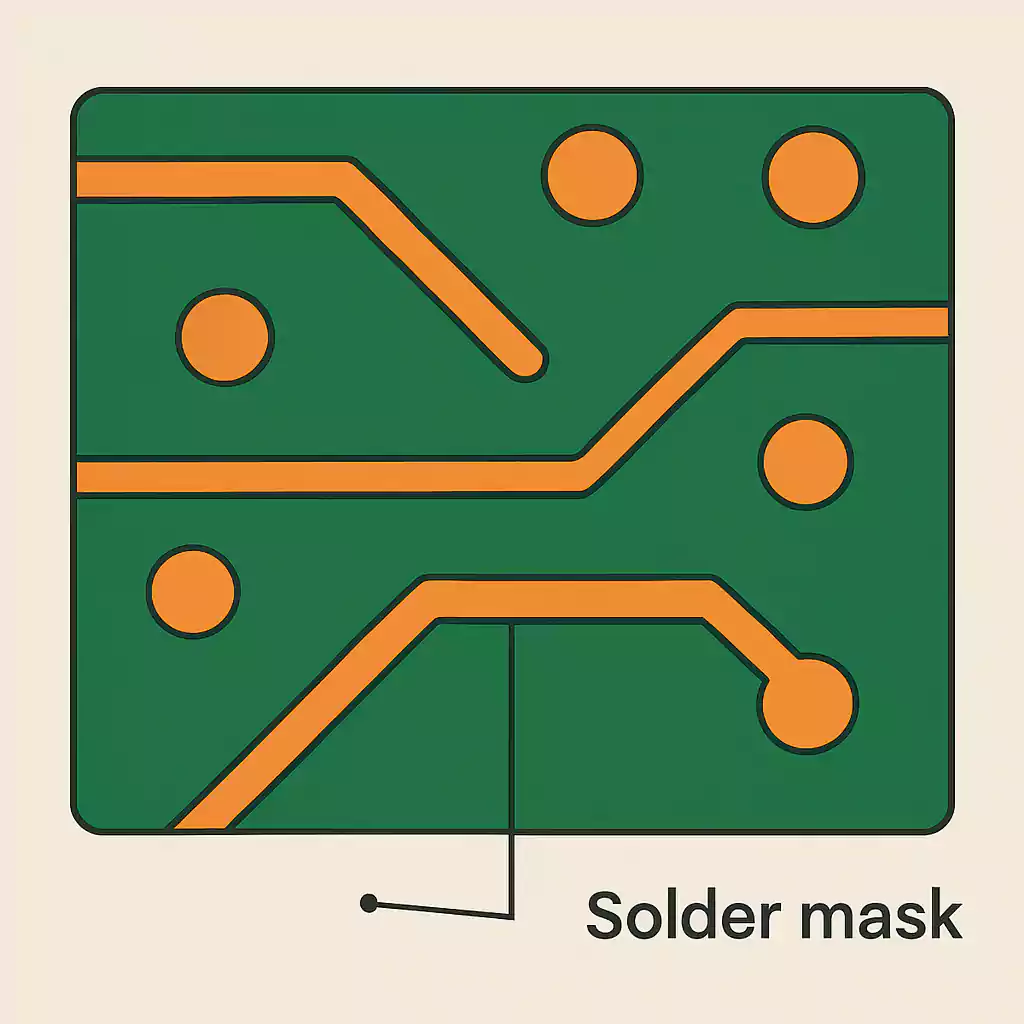
- Solder Mask: A protective layer placed over the copper to prevent oxidation and avoid solder bridges during assembly. It's usually green but can come in other colors.
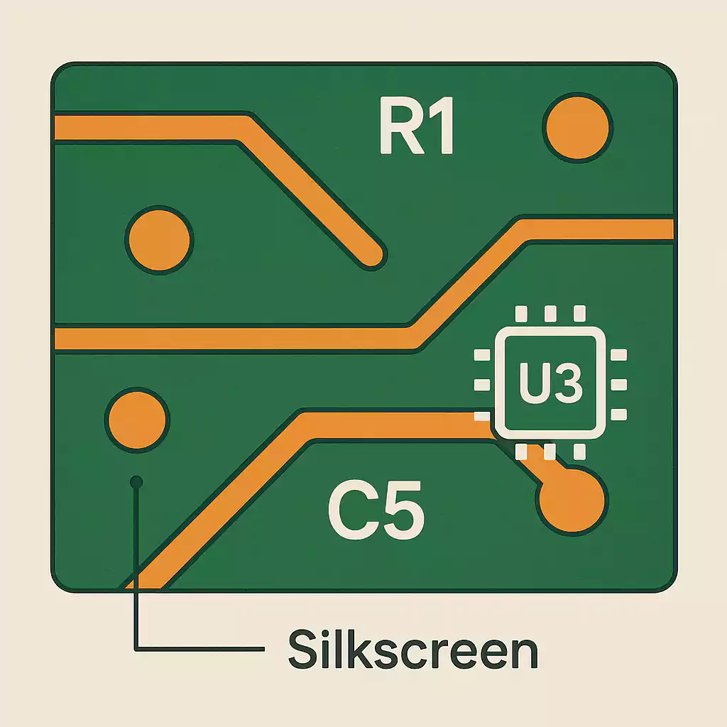
- Silkscreen: This topmost layer contains printed text and symbols to label components, test points, and other identifiers, aiding in assembly and troubleshooting.
Multi-layer PCBs may include inner copper layers, ground/power planes, and via connections that enable signal routing between layers.
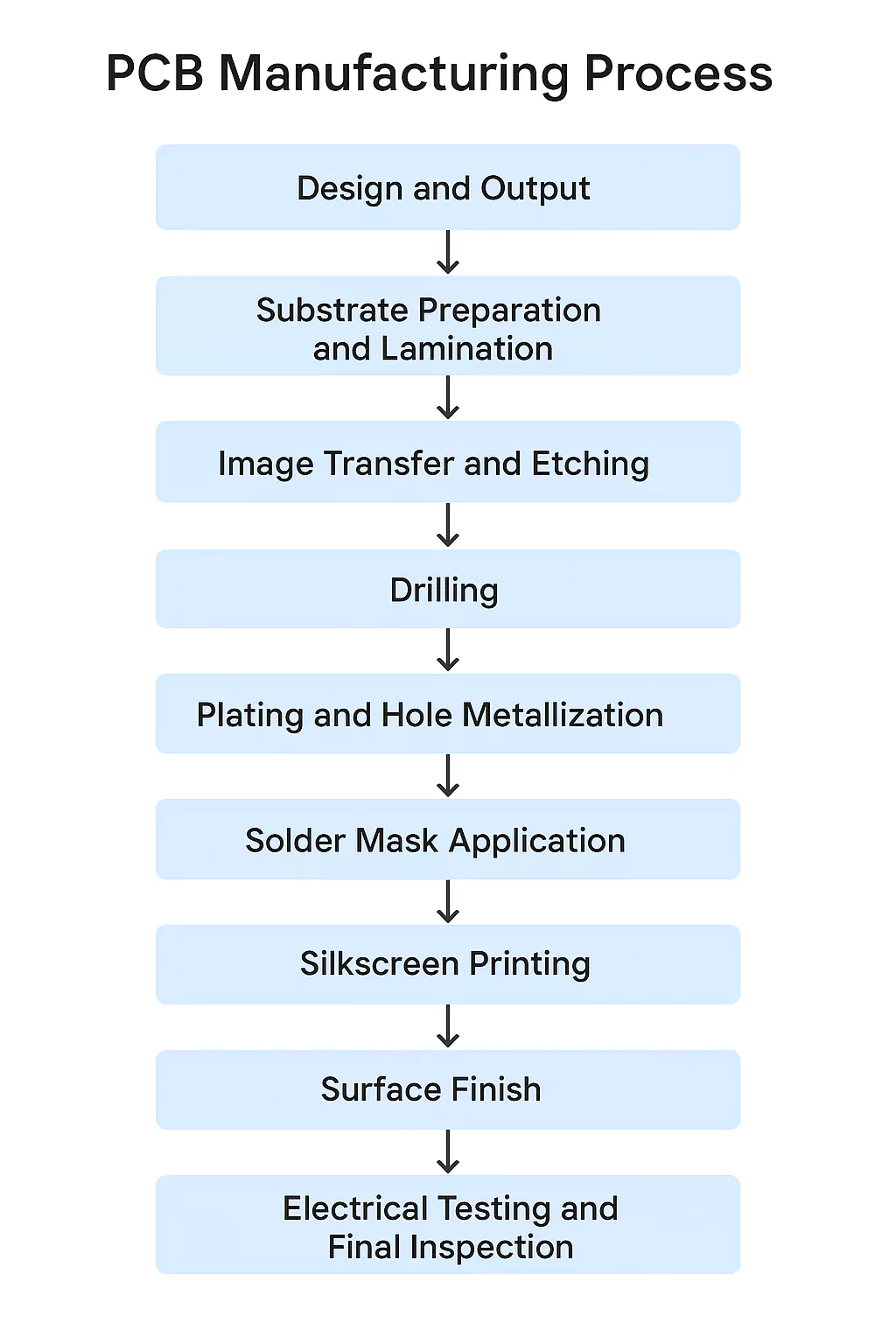
2. PCB Manufacturing Process: Step-by-Step
The PCB fabrication process is a precise series of chemical, mechanical, and thermal steps that transform raw materials into reliable circuit boards. Here's a simplified breakdown:
Step 1: Design and Output
The process begins with a PCB layout created using CAD software. The design files (Gerber files) define each layer's patterns and drill locations.
Step 2: Substrate Preparation and Lamination
Copper-clad laminates (typically FR4) are cleaned and prepared. For multi-layer boards, multiple layers are laminated together under heat and pressure.
Step 3: Image Transfer and Etching
The copper layers are coated with a photosensitive resist. The desired circuit pattern is exposed using UV light and then chemically etched to remove unwanted copper.
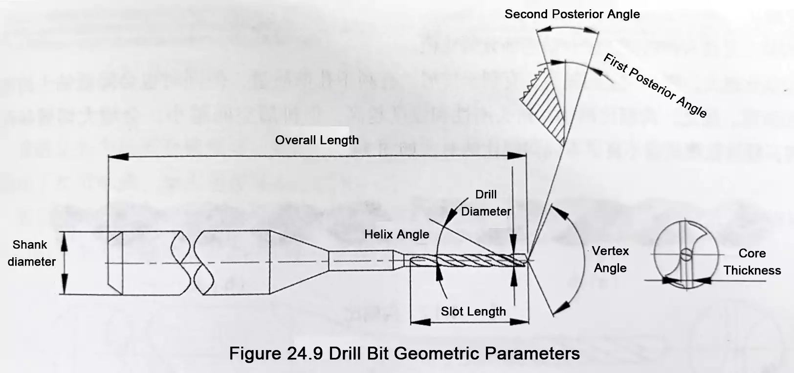
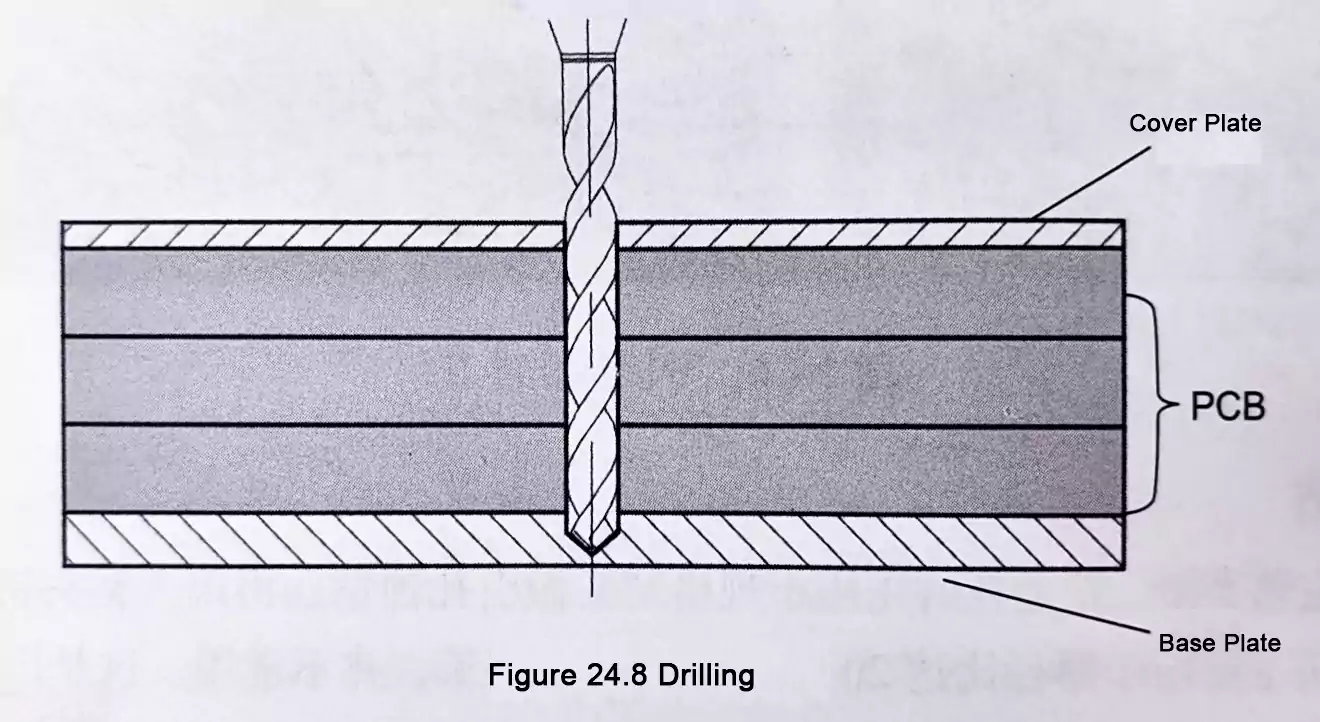
Step 4: Drilling
Precision drills create holes for vias and through-hole components. These holes are later plated to establish electrical connections between layers.
Step 5: Plating and Hole Metallization
Electroless copper plating deposits a thin layer of copper inside the drilled holes and on panel surfaces, enabling signal flow between layers.
Step 6: Solder Mask Application
The solder mask is applied to insulate the copper traces and define exposed areas for soldering.
Step 7: Silkscreen Printing
Text, logos, and component outlines are printed using the silkscreen layer to aid in assembly and inspection.
Step 8: Surface Finish
To enhance solderability and protect exposed copper, a surface finish is applied—options include HASL (Hot Air Solder Leveling), ENIG (Electroless Nickel Immersion Gold), and others.
Step 9: Electrical Testing and Final Inspection
Automated equipment tests the PCB for open circuits, shorts, and manufacturing defects before it's shipped for component assembly.
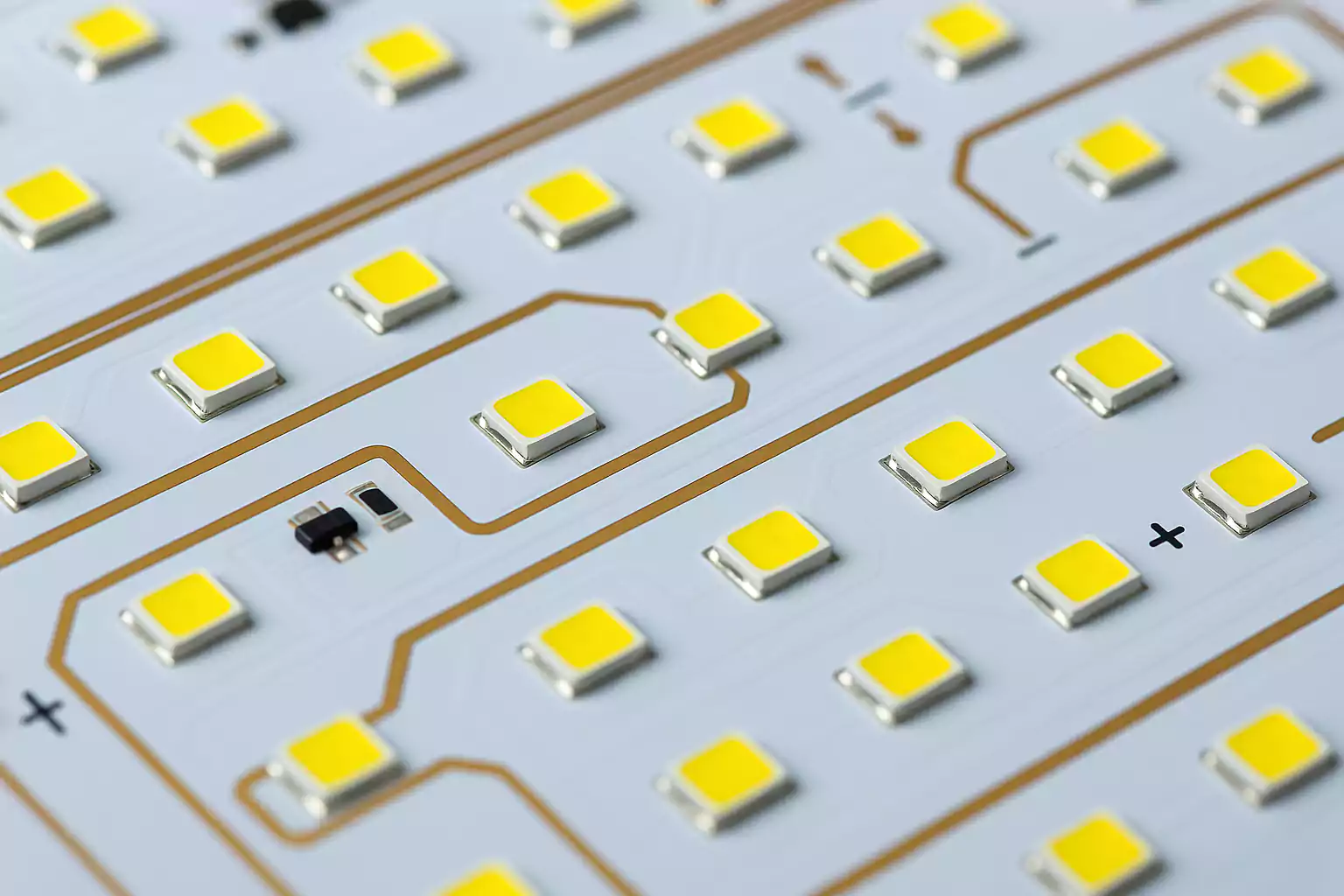
Passive Components on a PCB: Explained
Passive components are essential building blocks on any PCB. Unlike active components, they don't amplify signals or require external power to operate. Instead, they manage current, store energy, and filter signals within a circuit. Here are the most common passive components found on printed circuit boards:
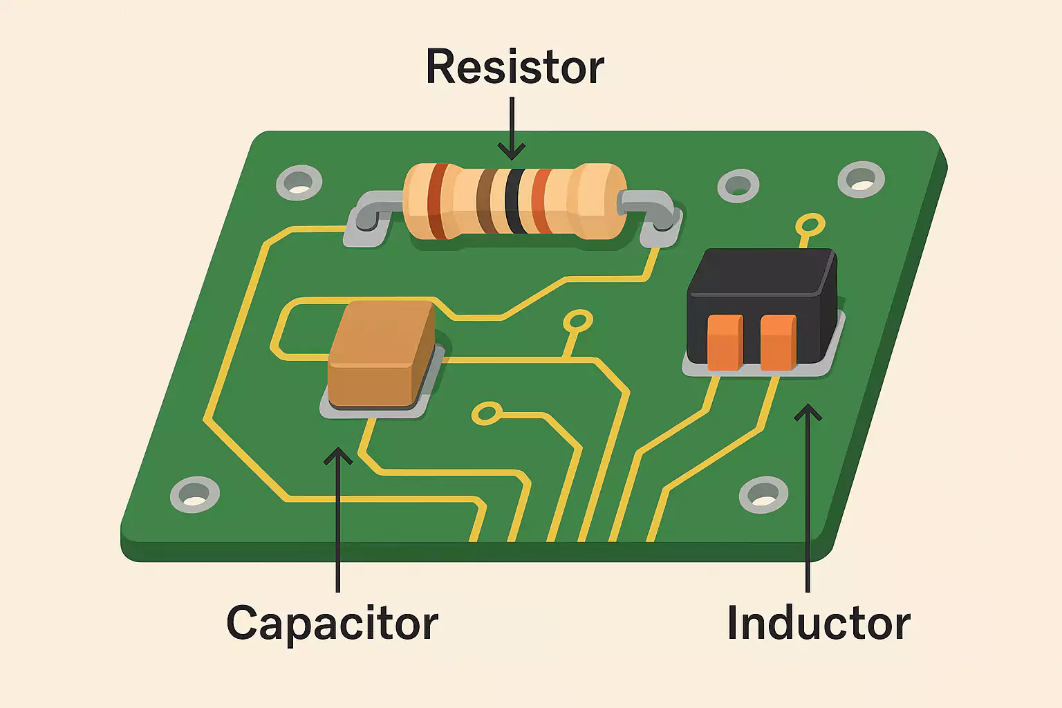
1. Resistors
Resistors limit the flow of electrical current and are used to control voltage levels, divide signals, and bias active components. They come in various types such as carbon film, metal film, and surface-mount resistors (SMD). When placing resistors on a PCB, consider their resistance value, tolerance, and power rating to ensure circuit stability.
2. Capacitors
Capacitors store and release electrical energy, acting as filters, timing elements, or decoupling agents. On PCBs, you'll commonly find ceramic, electrolytic, and tantalum capacitors. Ceramic capacitors are ideal for high-frequency decoupling, while electrolytic capacitors are often used for power supply filtering. Proper placement is key—especially for bypass and decoupling capacitors near ICs.
3. Inductors
Inductors resist changes in current and are used in power regulation, filtering, and energy storage. They are commonly found in DC-DC converters and RF circuits. When selecting inductors, important factors include inductance, current rating, and core material. On a PCB, they are typically larger than resistors or capacitors and may influence layout spacing.
4.Comparative Summary Table
| Component | Main Function | Typical Use Cases | SMD Available |
|---|---|---|---|
| Resistor | Limit current / divide volt. | LEDs, logic circuits, pull-up/down | ✅ Yes |
| Capacitor | Store & filter energy | Decoupling, power filtering | ✅ Yes |
| Inductor | Filter or store magnetic E | Power regulation, EMI suppression | ✅ Yes |
PCB Design Tip:
When working with passive components on a PCB, always consider signal integrity, thermal impact, and EMI sensitivity. Group related components (such as decoupling capacitors) close to their target ICs and minimize trace lengths to avoid performance issues.
Active and Semiactive Components Explained
1. Diodes
Function: Diodes are one-way valves for electrical current. They allow current to flow in a single direction, blocking reverse flow that could damage sensitive components.
Common Types:
- Rectifier Diodes: Convert AC to DC
- Zener Diodes: Provide voltage regulation
- Schottky Diodes: Offer fast switching and low voltage drop
- Applications: Power supplies, polarity protection, voltage clamping
2. Transistors
Function: Transistors act as electrical switches or amplifiers. They're fundamental to signal control and logic processing in modern electronics.
Types:
- Bipolar Junction Transistors (BJTs): Used for analog amplification
- Field-Effect Transistors (FETs): Preferred for switching and digital logic
- Use Cases: Motor drivers, logic gates, audio amplifiers, switching regulators
Design Tip: When using transistors on a PCB, consider heat dissipation and safe current limits to avoid thermal runaway.
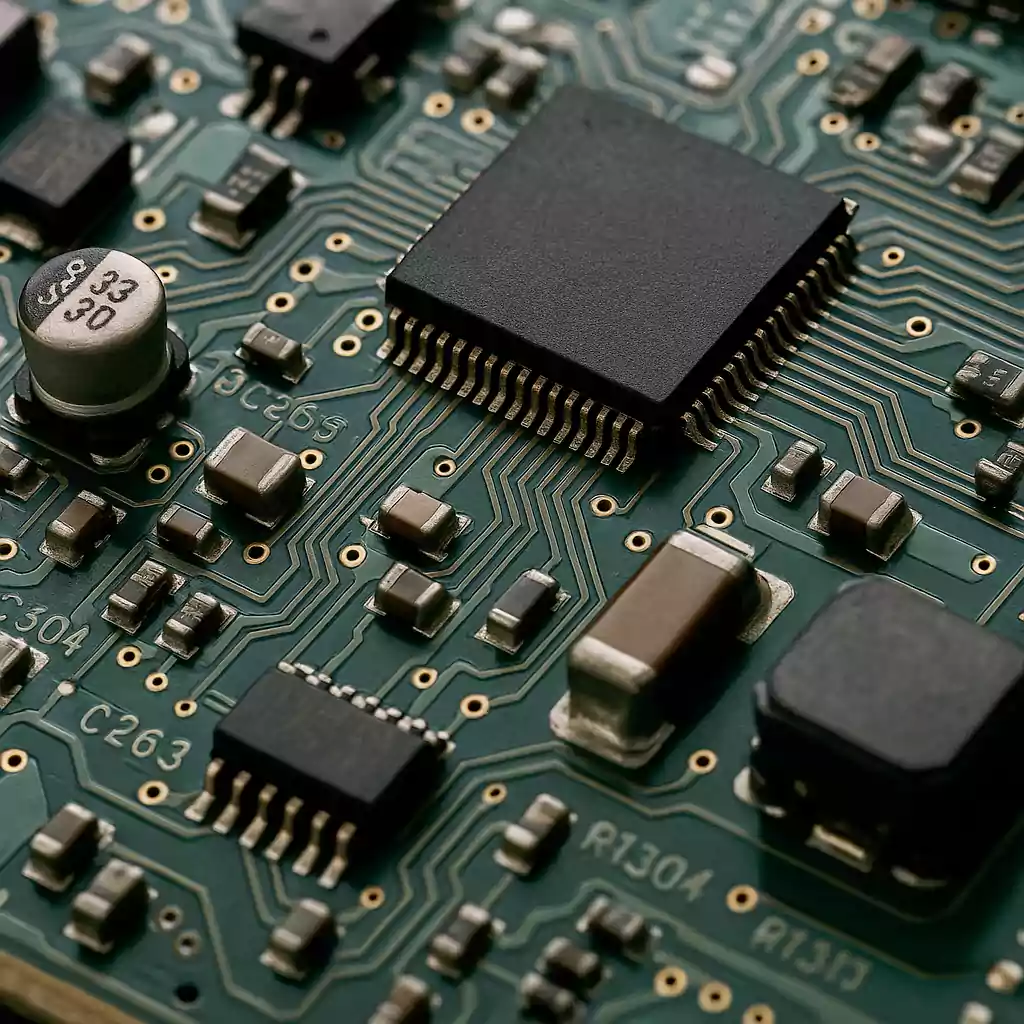
3. Integrated Circuits (ICs)
Function: ICs are compact packages that contain multiple components—transistors, resistors, capacitors—working together as a single system.
Categories:
- Analog ICs: Operational amplifiers, voltage regulators
- Digital ICs: Microcontrollers, logic gates, memory chips
- Mixed-Signal ICs: Combine analog and digital (e.g., ADCs, DACs)
- Advantages: Space-saving, high reliability, consistent performance
Example: A microcontroller (MCU) like the ATmega328 combines processing logic, timers, and I/O interfaces—all in one active component.
4. Crystal Oscillators
Function: Crystals generate precise clock signals for timing in microcontrollers and communication systems.
Key Characteristics:
- Stable frequency output
- Low power consumption
- High accuracy
Common Uses: Clocks for CPUs, communication modules (UART, SPI), and digital timing circuits
5. Semiactive Components Overview
Semiactive components are hybrids that exhibit both passive and active behavior. A good example is the photodiode, which conducts based on light exposure and often pairs with amplification circuitry. Others include varistors, thermistors, and opto-isolators.
While not strictly "active", these components are sensitive to external stimuli (light, temperature, voltage) and play critical roles in protection, detection, and signal conditioning.
Summary
Active and semiactive components are the decision-makers, amplifiers, and controllers of electronic circuits. They define how signals behave, how energy is directed, and how complex tasks are executed on the PCB. Understanding these components allows designers to build smarter, more efficient, and feature-rich systems.
Electromechanical Components and Interconnect Structures
Electromechanical components on a PCB serve as the critical bridge between electronic circuits and the physical world. These parts enable user interaction, mechanical mounting, power transfer, and data communication. Proper selection and placement of these components affect reliability, signal integrity, and manufacturability.
1.Connectors
Connectors are used to join PCBs with other boards, cables, or external devices. Common types include header pins, USB ports, edge connectors, FPC/FFC connectors, and board-to-board sockets. Selecting the right connector involves considering the number of pins, current rating, mechanical durability, and signal type (analog, digital, power). Poor connector quality or placement can lead to signal loss or mechanical failure, especially in high-vibration environments.
2.Switches
Switches provide manual control over circuit states—such as powering on a device or selecting a mode. Types include tactile switches, slide switches, toggle switches, and DIP switches. In PCB layouts, tactile switches are surface-mounted, while larger switches may be through-hole mounted for mechanical strength. Always check the switch's debounce characteristics and lifespan ratings.
3.Relays
Relays are electromechanical switches that use an electromagnet to control one or more electrical circuits. Though larger than semiconductor alternatives, they are useful in isolation, high-voltage switching, and automotive or industrial PCBs. PCB relays must be mounted with attention to heat and arc suppression requirements.
4.Interconnect Structures and Mechanical Integration
Beyond individual components, PCBs often include interconnect structures that support mechanical stability and multi-board assembly.
Key Elements:
- Board-to-Board Connectors: Stackable headers, mezzanine connectors
- Flex Cables / Ribbon Cables: Used for compact or moving designs (e.g., printers, wearables)
- Mounting Holes & Standoffs: Provide support and isolation from vibration or enclosure contact
- Shielding Cans / EMI Gaskets: Help reduce electromagnetic interference from high-speed components
Layout Tips:
- Keep mechanical clearance zones around mounting holes
- Use copper-free keep-out areas under standoffs to avoid shorts
- Maintain controlled impedance in interconnect regions for signal-critical lines
5.Summary Table: Electromechanical PCB Components
| Component | Function | Typical Use Case |
|---|---|---|
| Pin Header | Data/power board connection | Arduino shields, expansion modules |
| USB Connector | Data + power interface | Consumer devices, debug ports |
| Tactile Switch | Momentary user input | Reset buttons, UI interaction |
| Relay | Isolated high-power switching | Smart home, motor control |
| Edge Connector | Modular, slot-based connection | Graphics cards, memory modules |
| Mounting Hole | Mechanical support & grounding | All mechanical enclosures |
Special Structures in PCB: Footprints, Vias, Solder Mask, and Silkscreen
Beyond the electronic components themselves, a PCB is made up of several specialized structures that ensure electrical performance, manufacturability, and human readability. These include footprints, vias, solder masks, and silkscreen layers—each playing a vital role in how components are mounted, connected, protected, and identified on the board.
Understanding these elements is essential for high-quality PCB design and long-term product reliability.
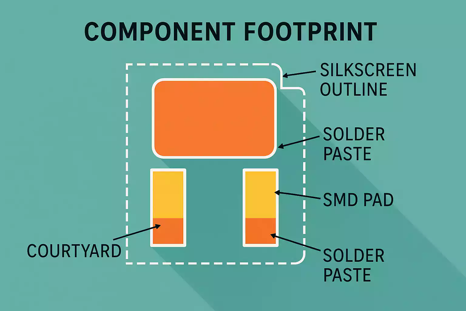
1. Footprints (Component Land Patterns)
Function: A footprint defines the physical layout of a component on the PCB, including pad sizes, spacing, hole dimensions, and outline markings.
What’s Included:
- SMD Pads or Through-Hole Pads
- Courtyard (clearance zone)
- Silkscreen Outlines and Pin 1 Indicators
- Solder Paste Layer (for stencil creation)
Why It Matters:
- Incorrect footprints lead to mounting errors, soldering defects, and field failures.
- Following standards like IPC-7351 ensures compatibility with pick-and-place machines and reflow processes.
Always match your footprint to the exact package used (e.g., SOIC-8 vs. TSSOP-8), and simulate for solder pad alignment.
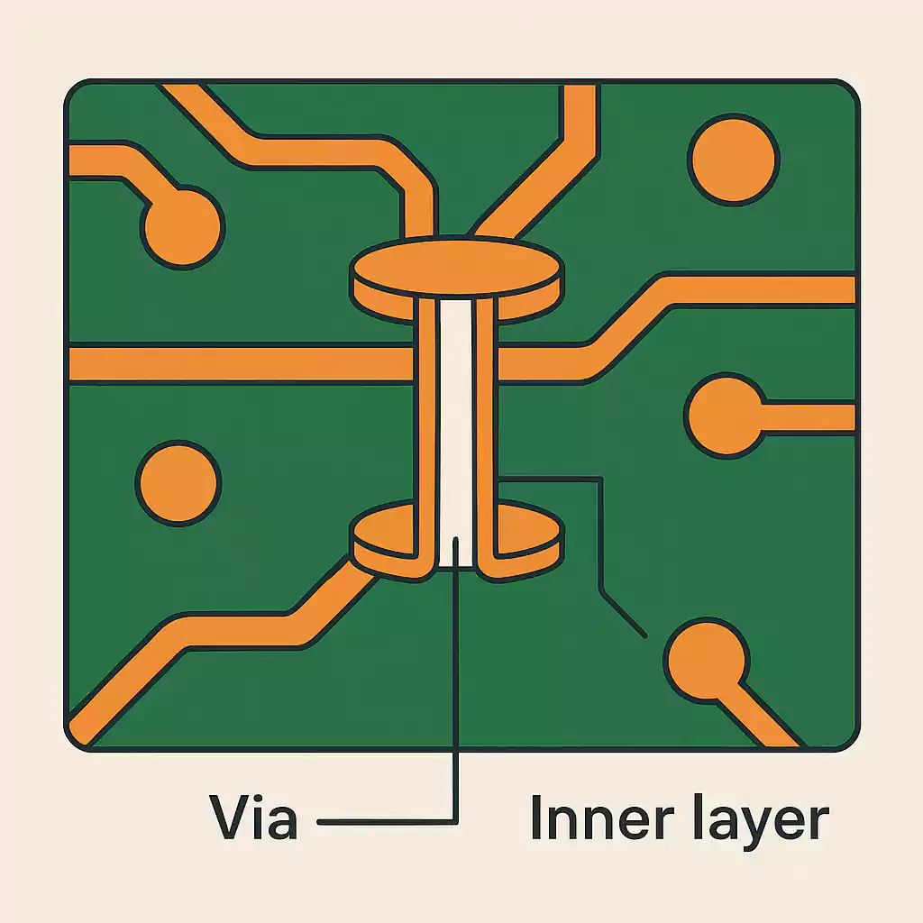
2. Vias (Vertical Interconnect Access)
Function: Vias connect copper layers in a multi-layer PCB. They allow signals and power to travel between top, inner, and bottom layers.
Types of Vias:
- Through-Hole Via: Drilled through the entire board; most common and cost-effective.
- Blind Via: Connects an outer layer to an inner layer—saves space in dense layouts.
- Buried Via: Connects only internal layers—used in HDI (High-Density Interconnect) boards.
- Microvia: Laser-drilled, very small vias often used in mobile devices and high-frequency designs.
Design Considerations:
- Thermal Relief: Prevents overheating during soldering.
- Via-in-Pad: Useful for BGA packages but requires via filling and planarization.
For high-speed designs, minimize via stubs and ensure controlled impedance paths through careful stackup design.
3. Solder Mask
Function: The solder mask is a protective polymer layer applied over the copper traces, preventing solder bridges, oxidation, and environmental damage.
Characteristics:
- Typically green (but also available in red, black, white, blue, etc.)
- Exposes only the necessary pads or vias for soldering
- Enhances electrical insulation and product lifespan
Design Tips:
- Ensure solder mask clearance around small pitch pads (like QFNs or BGAs)
- Avoid overlapping the solder mask with exposed copper traces
A well-defined solder mask improves automated assembly yield and protects against short circuits during handling.
4. Silkscreen (Legend Layer)
Function: The silkscreen is a printed layer used to identify components, test points, logos, pin 1 indicators, and orientation marks.
Key Elements:
- Reference designators (e.g., R1, C5, U2)
- Polarity indicators for diodes and capacitors
- Manufacturer logos, part numbers, or QR codes
Application Methods:
- Inkjet printing (modern, fine-pitch friendly)
- Screen printing (traditional, more durable)
Best Practices:
- Avoid placing silkscreen under components
- Maintain legible font size (≥0.8 mm height recommended)
- Use contrasting ink color for readability
The silkscreen layer greatly improves repairability, manual inspection, and assembly processes.
5. Quick Comparison Table
| Structure | Function | Design Consideration |
|---|---|---|
| Footprint | Mount and align components | Match package type and IPC standard |
| Via | Interconnect between PCB layers | Type selection based on space and signal path |
| Solder Mask | Protect traces, define solder areas | Proper clearance, avoid pad coverage |
| Silkscreen | Label and identify components | Font size, placement, orientation |
Signal Integrity and Thermal Management Design
As PCB designs grow faster and denser, maintaining signal integrity and implementing effective thermal management become critical to ensuring reliability, performance, and compliance with regulatory standards. Poor handling of either can result in data corruption, excessive noise, system instability, or even hardware failure.
This section breaks down the key principles and best practices for optimizing high-speed signal behavior and managing heat dissipation in PCB layouts.
1. What Is Signal Integrity?
Signal integrity (SI) refers to the quality and stability of electrical signals as they travel across the PCB. In high-frequency circuits, signals behave more like electromagnetic waves than simple voltage levels. Issues such as reflection, crosstalk, ringing, and impedance mismatch can distort signals and degrade performance.
Key Factors That Affect Signal Integrity:
- Impedance Discontinuity: Caused by inconsistent trace width, via transitions, or poor stackup.
- Long Trace Lengths: Act as transmission lines and introduce delay and reflections.
- Poor Grounding or Power Distribution: Leads to voltage drops and increased noise.
- Via Stubs: Unused via branches act like antennas, disrupting signal timing.
Best Practices for Signal Integrity in PCB Design:
- Use controlled impedance traces for high-speed signals (e.g., USB, HDMI, DDR).
- Keep return paths short and continuous, using solid ground planes.
- Match trace lengths in differential pairs and clock/data lines to avoid skew.
- Minimize the number of vias in critical signal paths.
- Add termination resistors where needed to prevent reflections.
Tip: Use impedance calculators and field solvers (e.g., Saturn PCB Toolkit, Altium, or Polar Si9000) during layout design.
2. Understanding Thermal Management in PCBs
Thermal management ensures that heat generated by components and signal losses does not exceed safe operating temperatures. Excessive heat shortens component life, affects performance, and can lead to failure of solder joints or PCB material delamination.
Primary Heat Sources in a PCB:
- Power semiconductors (MOSFETs, regulators, CPUs)
- High-current traces or planes
- Dense BGA packages or RF modules
3.Key Techniques for Effective PCB Heat Dissipation:
a. Copper Area and Planes
- Use large copper pours around high-power components.
- Employ internal ground or power planes as heat sinks.
b. Thermal Vias
- Place thermal vias beneath hot components to conduct heat to inner or bottom layers.
- Use via arrays (filled or unfilled) to transfer heat through multiple layers efficiently.
c. Heatsinks and Heat Spreaders
- Attach external heatsinks or metal slugs for components with high thermal output.
- Use thermal pads and interface materials to enhance heat transfer.
d. PCB Material Selection
- Choose high-Tg FR4 or metal-core PCB (MCPCB) for demanding thermal applications like LED drivers or power converters.
e. Component Placement
- Isolate heat-sensitive components from heat sources.
- Avoid placing high-power parts near the PCB edge unless a heatsink is attached.
Rule of Thumb: Keep junction temperature (Tj) under 125°C for most components—use datasheet thermal resistance (θJA) and power dissipation values to estimate thermal loads.
4.Signal and Thermal Design Go Hand-in-Hand
Signal integrity and thermal management often conflict—e.g., large ground pours help thermal conduction but may introduce unwanted impedance changes. A balanced design accounts for both by:
- Designing solid, low-inductance return paths for signals
- Combining thermal and electrical vias under BGA pads
- Using split planes with caution to avoid creating noisy return loops
Summary Table: Signal vs. Thermal Design Goals
| Design Concern | Signal Integrity Goal | Thermal Management Goal |
|---|---|---|
| Trace Design | Controlled impedance, minimal reflections | Wider traces for current carrying |
| Via Usage | Fewer stubs, matched lengths | Multiple vias for thermal transfer |
| Plane Strategy | Unbroken return paths, low noise | Large copper pours for heat spreading |
| Component Placement | Short, direct signal routes | Thermal isolation and sink accessibility |
Real-World Case Study: PCB Component Selection in Electronic Products
Component selection isn't just about datasheets—it's about matching function, form, and performance to the product's specific needs. In this section, we'll compare how components are chosen differently in three common types of electronics: a smartphone motherboard, a power supply module, and an LED lighting controller.
Here's how professionals adapt their PCB component selection strategies based on electrical, thermal, and mechanical requirements:
Comparison Table: PCB Component Choices by Application
| Component Type | Smartphone Motherboard | Power Supply Module | LED Lighting Controller |
|---|---|---|---|
| Microcontroller / SoC | High-integration SoC with embedded wireless (e.g., Snapdragon) | Minimal or none; often uses analog control | Low-power MCU (e.g., STM32, ATtiny) for dimming |
| Power Regulation | PMICs with buck-boost converters & LDOs | High-current switching regulators (DC-DC, flyback) | Linear regulators or small buck converters |
| Capacitors | Low-ESR MLCCs for decoupling near ICs | High-value electrolytics for input/output filtering | Ceramic + electrolytic combo for cost/stability |
| Resistors | High-density SMD resistors (0402, 0201) | 1% tolerance, higher power rating (e.g., 0.25W) | Through-hole or 1206 SMD for reliability |
| Inductors | Shielded low-profile inductors for space | Large power inductors (ferrite core) | Small inductors for buck dimmers |
| Connectors | FPC/BTB for internal modules, USB-C ports | Screw terminals or barrier blocks | JST or screw terminals for easy wiring |
| Display Interface | MIPI-DSI or eDP with ESD protection | Not applicable | May use simple LED indicators or 7-segment display |
| Thermal Design | Heat spreaders, graphite films, thermal vias | Thick copper pours, external heatsinks | Mid-level thermal pads under MOSFETs |
| PCB Type | HDI multilayer (6–12 layers) | Double-sided or 2–4 layer, FR4 or CEM-1 | Single or double-sided, FR4 or aluminum-based |
| Cost Sensitivity | High-performance, less price-sensitive | Mid-range BOM optimization | Cost-sensitive; focus on reliability |
Insights and Takeaways
- Smartphones prioritize size and integration: Space-saving, high-performance components are key. Every passive must be small (0201/01005), and power is tightly managed.
- Power modules prioritize durability and thermal handling: Inductors, capacitors, and MOSFETs are chosen for thermal endurance and EMI suppression, not size.
- LED controllers balance cost and robustness: Designers often select cost-effective through-hole components for better thermal performance and field replaceability.
By studying real-world PCB component choices, engineers can learn how to adjust their designs for cost, size, function, and environment—ensuring their products are optimized from both an electrical and manufacturing standpoint.
Common Engineering Mistakes & Best Practices in PCB Design
Even experienced engineers can fall into common pitfalls when designing printed circuit boards. Small oversights in layout, component placement, grounding, or thermal considerations can lead to product failures, EMI issues, or manufacturing defects. This section outlines the most frequent PCB design mistakes and the proven best practices to avoid them.
Common PCB Design Mistakes
| Mistake | Description | Impact |
|---|---|---|
| Inadequate Grounding | Broken or narrow ground paths; split planes | Causes EMI, noise, and poor signal return |
| Via Overuse in High-Speed Signals | Excessive or improperly placed vias on critical signal paths | Signal distortion, reflections |
| Poor Component Placement | Randomized layout, long traces between related components | Increases EMI, trace delay, heat buildup |
| Thermal Hotspots Ignored | Placing power components without thermal relief | Overheating, reduced component lifespan |
| No Design for Manufacturability (DFM) | Pads too small, silkscreen over pads, irregular footprints | Assembly errors, increased production cost |
| Not Following IPC Standards | Non-standard pad sizes, trace clearances, or via arrangements | Reliability issues, failed fab checks |
| Missing Test Points | No access for probes or automated testing | Difficult debugging and QA testing |
| Trace Width Too Narrow | Especially for power or high-current lines | Overheating, copper trace burnout |
| Unmatched Differential Pairs | Uneven trace lengths in clock or high-speed data pairs | Skew and timing failures |
| Neglecting EMC/EMI Controls | No shielding, poor layout of high-frequency components | Signal leakage, regulatory test failures |
PCB Design Best Practices
| Best Practice | Why It Matters |
|---|---|
| Use Solid Ground and Power Planes | Ensures low-impedance return paths and EMI immunity |
| Apply Controlled Impedance Design | Essential for USB, HDMI, Ethernet, and other high-speed interfaces |
| Thermal Via Arrays under Hot Components | Improves heat dissipation to inner/bottom layers |
| Group Related Components Together | Minimizes trace length and improves routing efficiency |
| Use Design Rule Checks (DRC) & ERC Tools | Automated checks catch violations before fabrication |
| Adopt Standard Footprints (IPC-7351) | Ensures manufacturability and reliability |
| Plan for Test Points Early | Simplifies debugging, programming, and QA processes |
| Use Decoupling Capacitors Strategically | Placed close to IC power pins for clean power delivery |
| Simulate Signal and Thermal Behavior | Tools like SPICE and thermal analyzers validate before manufacturing |
| Document Everything Clearly | Schematics, silkscreen, BoM, and layout notes help ensure design continuity |
Bonus Tips for Reliable PCB Development
- Collaborate with your manufacturer during layout to align with their fabrication capabilities.
- Always review layer stackups and material choices for thermal and high-speed needs.
- Run a full Design for Assembly (DFA) and Design for Test (DFT) review before finalizing production files.
- Use 3D PCB visualization tools to catch enclosure conflicts or alignment issues.
- Include assembly notes, mechanical dimensions, and special handling instructions in your documentation package.
Conclusion & Call to Action
Printed circuit boards are more than just a platform for connecting parts—they are the heart of every electronic system. From passive components like resistors and capacitors to advanced active ICs, electromechanical connectors, and critical structures such as vias and solder masks, each element plays a vital role in determining the reliability, performance, and manufacturability of a product.
By understanding the components of a PCB and how they interact with board structure, thermal behavior, and signal paths, engineers and makers alike can build smarter, safer, and more cost-effective designs. Whether you're prototyping a new product or optimizing a mass-manufactured board, applying the best practices in component selection, layout, and thermal/signal design is key to long-term success.
Ready to Build Better PCBs?
- Bookmark this guide as your go-to PCB component reference
- Apply the checklists and comparison tables to your next design project
- Have a question or feedback? Leave a comment or join our community discussion
- Download our free PCB layout checklist and component selection worksheet
- Subscribe to our newsletter for advanced PCB design tips, tools, and trends
Looking to take your circuit board design skills to the next level? Stay informed, keep learning, and always test before you build.
Your next great hardware product starts with the right components—and this guide is your foundation.