


Introduction
As PCB designs become increasingly compact and complex, traditional manual inspection methods struggle to keep pace with modern manufacturing demands. Fast production cycles and shrinking component sizes increase the risk of undetected defects, leading to costly rework or product failure.
Automated Optical Inspection (AOI) addresses this challenge by using high-resolution cameras and image processing software to quickly and accurately detect surface defects on PCBs. AOI plays a critical role in maintaining quality, improving yield, and reducing costs in today’s electronics production lines.
In this guide, you’ll learn what AOI is, where it fits in the PCB manufacturing process, what defects it detects, how it compares to other inspection methods, and how it supports long-term quality and productivity goals.
What Is AOI?
Automated Optical Inspection (AOI) is a non-contact, camera-based inspection technique used in PCB manufacturing to detect visual defects during both the fabrication and assembly stages. By scanning each circuit board with high-resolution cameras under controlled lighting conditions, AOI systems can quickly identify issues such as:
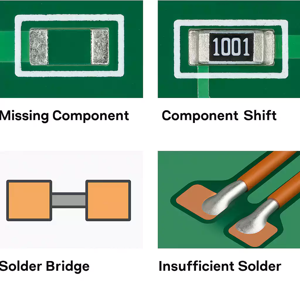
- Missing or misaligned components
- Solder bridges or insufficient solder
- Scratches, stains, or foreign objects
- Open circuits and short circuits
- Polarity or orientation errors
Unlike manual inspection, which is labor-intensive and prone to inconsistencies, AOI delivers fast, repeatable, and highly accurate results—making it essential for high-volume or high-reliability production environments.
During production, a reference image—often referred to as a “golden board”—is used as the baseline. AOI systems compare real-time images of each board against this reference or directly against the design files (CAD or Gerber data). Any deviation is flagged as a potential defect and reviewed by technicians for confirmation and corrective action.
By catching defects early in the process—typically right after component placement or reflow soldering—AOI helps manufacturers reduce scrap, minimize rework, and maintain high-quality standards across every production run.
AOI Technology and Workflow in PCB Manufacturing
1. Where AOI Fits in the PCB Production Line
AOI systems are strategically placed at multiple points along the PCB manufacturing and assembly process to ensure early and accurate defect detection. The typical workflow includes:
- Post-Solder Paste Inspection (SPI Alternative): Some manufacturers use AOI after solder paste printing to verify stencil alignment and paste volume.
- Post-Component Placement (Pre-Reflow AOI): AOI checks for missing, misplaced, or misaligned components before they are soldered. Catching errors here avoids wasteful soldering of defective assemblies.
- Post-Reflow AOI: After reflow soldering, AOI inspects for solder joint defects, including bridges, insufficient solder, tombstoning, and open joints.
- Bare Board AOI (for PCB Fabricators): In PCB fabrication, AOI is also used to inspect etching quality, shorts, opens, and registration errors before the boards are assembled.
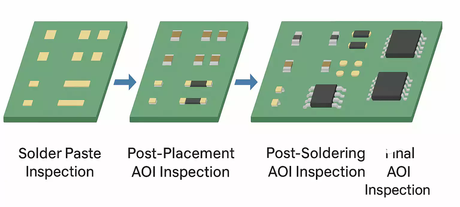
This staged inspection approach ensures quality control at every critical step, reducing the likelihood of defects being passed downstream.
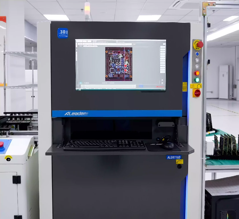
2. Key Components of an AOI System
AOI machines combine precision hardware and intelligent software to deliver high-speed, high-accuracy inspections. The major components include:
- High-Resolution Cameras: Capture detailed images of the PCB surface from multiple angles. In 3D AOI systems, structured light is used to measure component height and the volume of solder.
- Lighting System: Carefully calibrated lighting (top-down, side, ring, and multi-angle LED sources) enhances defect visibility by reducing glare and shadow.
- Image Processing Software: Compares captured images against reference data, either a “golden board” or CAD/Gerber files, using pattern recognition, color matching, and geometric analysis.
- Conveyor and Positioning System: Precisely moves and aligns the PCB under the inspection head to ensure full surface coverage.
Together, these components enable AOI to detect a wide range of manufacturing defects with remarkable speed and accuracy.
3. 2D vs. 3D AOI: Which One Do You Need?
There are two main types of AOI systems used in PCB production:
- 2D AOI: Uses flat images to detect defects related to component placement, polarity, orientation, and solder bridging. It is fast and cost-effective for general surface inspections.
- 3D AOI: Utilizes depth measurement techniques such as structured light or laser triangulation, making it ideal for inspecting solder joint volume, height, and coplanarity. This is especially important for fine-pitch components, such as BGAs or QFNs.
For high-density or mission-critical PCBs, 3D AOI offers a more reliable assessment of solder quality, thereby reducing false calls and enhancing process control.
4. Practical Deployment Considerations
Successfully integrating AOI into your production line requires attention to both technical specs and operational needs:
- System Selection: Choose a system that matches your production speed, component density, and defect types. Consider inspection resolution, camera speed, software flexibility, and ease of programming.
- Programming and Calibration: Define defect criteria and acceptable tolerances based on your product and IPC standards. Optimize lighting profiles and inspection angles for different board layouts.
- MES Integration: For smart factories, AOI systems can be connected to Manufacturing Execution Systems (MES) for real-time defect tracking, SPC analysis, and traceability.
- Operator Training: Proper training ensures consistent interpretation of AOI results, minimizes false positives, and improves response time for corrective action.
When properly deployed, AOI becomes more than a defect detector—it becomes a data-driven quality management tool.
The Business Value of AOI in PCB Manufacturing
1. Improve Quality, Reduce Rework
Automated Optical Inspection (AOI) significantly improves product quality by detecting defects—like missing parts, misalignment, or solder issues—early in the production process. This reduces rework, minimizes defective shipments, and increases first-pass yield.
Compared to manual inspection, AOI provides higher accuracy and consistency, especially for high-density or high-volume PCB production.
2. Lower Costs, Boost Efficiency
AOI reduces overall manufacturing costs by:
- Minimizing scrap and repair labor
- Replacing or supporting manual inspection
- Increasing inspection speed and throughput
Most manufacturers see a return on investment (ROI) within 6–12 months, especially when operating at medium to high volume.
3. Traceability and Compliance
AOI systems automatically log inspection data, including defect images and pass/fail records. This ensures:
- Full traceability for internal audits or customer reporting
- Easier compliance with IPC, ISO, automotive, or medical standards
AOI vs Other PCB Inspection Methods: Comparison Table
| Method | Type | Detects | Strengths | Limitations |
|---|---|---|---|---|
| AOI | Optical (2D/3D) | Surface defects: missing parts, misalignment, solder bridges | Fast, accurate, non-contact | Cannot inspect hidden solder joints |
| AXI | X-Ray | Hidden defects: BGA voids, internal shorts | Internal inspection, essential for BGA | Slower, more costly |
| ICT | Electrical Test | Opens, shorts, wrong component values | High test coverage, electrical validation | Requires test fixtures, no visual data |
| Functional Test | End-Use Simulation | Real-world circuit behavior | Final validation, system-level check | Doesn’t pinpoint physical defects |
| SPI | Optical | Solder paste volume, misalignment | Early detection, improves reflow quality | Limited to pre-placement stage |
Technology Trends and Future Outlook for AOI
- AI-Powered Inspection
Next-generation AOI systems are integrating machine learning to reduce false calls, improve adaptability, and enable continuous performance optimization.
- Industry 4.0 Integration
AOI now functions as a real-time data source, feeding defect data into MES/SPC systems to support automated traceability, process control, and predictive quality.
- Precision for Miniaturization
To meet the demands of HDI, BGA, and 01005 components, AOI systems are advancing with higher-resolution optics and enhanced 3D measurement capabilities.
- Sustainability Support
By reducing scrap and enabling process efficiency, AOI contributes to sustainable electronics manufacturing and supports ESG initiatives.

Conclusion
Automated Optical Inspection (AOI) is a key quality control tool in modern PCB manufacturing. It enables fast, accurate defect detection, helping reduce rework, improve yield, and ensure consistent product quality.
As demands for precision and traceability continue to grow, AOI is evolving—integrating with smart factory systems and leveraging AI for enhanced performance. For manufacturers looking to stay competitive, AOI is not just an inspection step but a strategic component of a reliable and efficient production process.