

In electronics, amplifiers are everywhere—from audio systems and communication modules to RF transmitters and even guitar pedals. The printed circuit board (PCB) behind an amplifier determines how well that circuit performs.
A well-designed amplifier PCB circuit minimizes noise, prevents oscillation, and delivers stable gain. A poor one, on the other hand, can easily cause distortion, hum, or overheating.
What Is an Amplifier PCB Circuit?
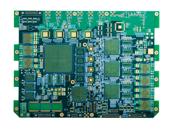
An amplifier PCB circuit is the physical implementation of an amplifier on a printed circuit board. It contains all the active and passive components that increase the strength of an electrical signal.
In an amplifier PCB, three main areas exist:
- Input stage – Handles weak signals and needs clean, low-noise routing.
- Power/output stage – Delivers current to the load (speakers, antennas, etc.).
- Power supply and grounding – Feeds energy to the system and manages return paths.
The main goal is to transfer power or voltage gain from the input to the output while keeping the signal clean. A good PCB layout ensures that current loops are small, heat is managed, and noise doesn’t sneak into the signal path.
Key Components and Selection Tips
Active Components
- Operational amplifiers (op-amps) or audio amplifier ICs are the heart of the circuit. Choose parts with proper bandwidth, slew rate, and noise performance for your application.
- Transistors (BJT or MOSFET) are often used in power stages. BJTs offer linear gain, while MOSFETs provide efficiency and fast switching for Class-D designs.
Passive Components
- Resistors and capacitors define gain, feedback, and frequency response. Always use precision components for feedback networks to maintain stability.
- Inductors and EMI filters help suppress switching noise in power or Class-D amplifiers.
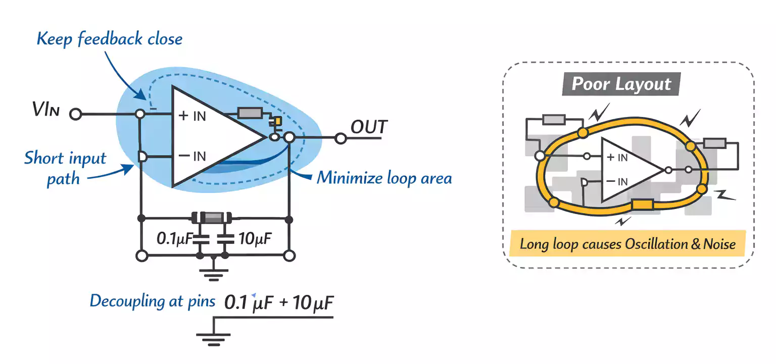
- Keep traces between feedback components as short as possible—long routes can cause phase shift and oscillation.
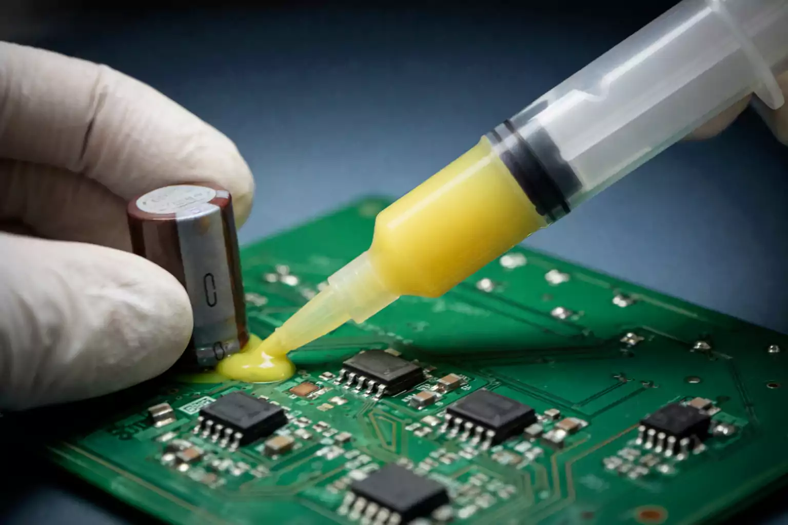
Thermal and Mechanical Parts
Amplifiers generate heat, especially power types. Use:
- Wide copper areas under power devices.
- Thermal vias to connect to internal planes or the opposite side of the board.
- Heatsinks or metal enclosures, if needed.
Good thermal design improves both reliability and sound quality.
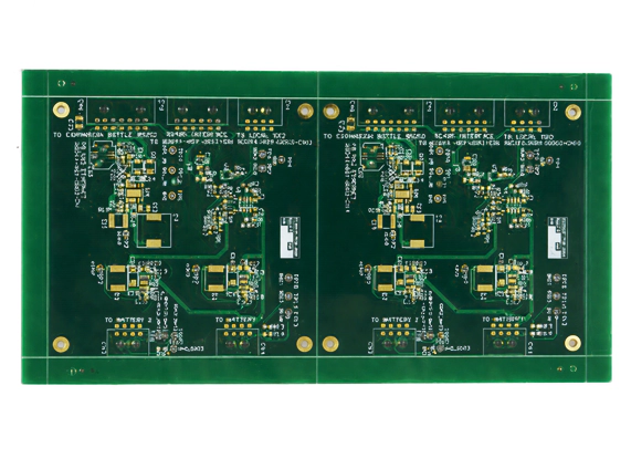
The Seven Golden Rules of Amplifier Layout
1. Keep Signal Paths Short
The smaller the loop, the less noise you pick up. Place input, feedback, and gain-setting components close to the IC pins. Avoid running sensitive traces through noisy areas, such as power or switching regions.
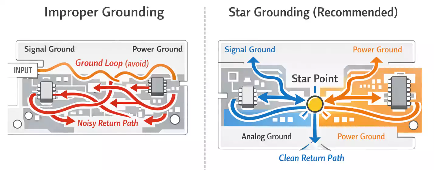
2. Ground Separation and Star Grounding
Separate analog, digital, and power grounds. Use a star-ground connection, where all sections meet at a single point near the power input. This prevents ground loops that create hum in audio amplifiers.
3. Power and Ground Planes
Use solid copper planes instead of thin traces for power and ground. They reduce impedance and improve stability. If your PCB includes both analog and digital circuits, divide the planes and connect them to a single point of control.
4. Routing Geometry
Avoid 90-degree corners—use 45-degree bends for smoother current flow and less EMI. Keep high-current traces wide, and ensure sensitive lines (like feedback) don’t cross power traces.
5. Minimize Loop Area in Feedback and Input Circuits
The feedback loop should be compact, ideally surrounding the op-amp or driver. A large loop area acts like an antenna, introducing noise and instability.
6. Local Decoupling—Small, Medium, Large
Every active device needs capacitors close to its power pins:
- 0.1 µF ceramic (high-frequency)
- 1 µF to 10 µF ceramic or tantalum (mid-frequency)
- 100 µF electrolytic (low-frequency bulk)
Place them as close as possible to the pins, with short traces to ground.
7. Thermal and EMI Considerations
Group high-current paths together and avoid overlapping with sensitive analog areas. Use copper pour and thermal vias to distribute heat. For Class-D or RF amplifiers, consider adding a grounded shield can over noisy sections.
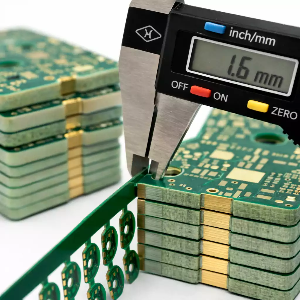
Routing and Layer Stackup
Recommended Layer Counts
- Single-sided or double-layer boards work for low-power audio and simple op-amp circuits.
- Four or more layers are recommended for high-speed or switching amplifiers, as they provide dedicated ground and power planes.
Network Priority
When routing:
- Feedback and input paths come first.
- Then local decoupling and power traces.
- Finally, control or low-priority signals.
Vias and Layer Transitions
Each via adds inductance. Keep high-frequency or feedback signals on one layer when possible. When crossing layers, ensure the reference ground plane remains continuous under the trace. Never route sensitive lines across gaps in the ground plane.
Power Integrity and Decoupling in Practice
Noise in the power supply can directly modulate your amplifier’s output. Clean power means clean sound.
Filtering
Use a combination of bulk capacitors and LC filters at the supply input to block ripple and switching noise. A π-filter (capacitor-inductor-capacitor) is common in audio or RF circuits.
Placement
Place the smallest capacitors closest to the power pin, then medium and large ones farther out. The return path of each capacitor should connect directly to the same ground plane or pad as the IC, not through long traces.
Measurement and Debug
When checking noise on an oscilloscope, use a short ground spring or coaxial probe. Long ground leads can act like antennas, leading to misleading results.
Thermal Design and Reliability
Amplifiers can run hot, especially in continuous or high-power operation. Thermal management keeps them reliable and prevents distortion caused by temperature drift.
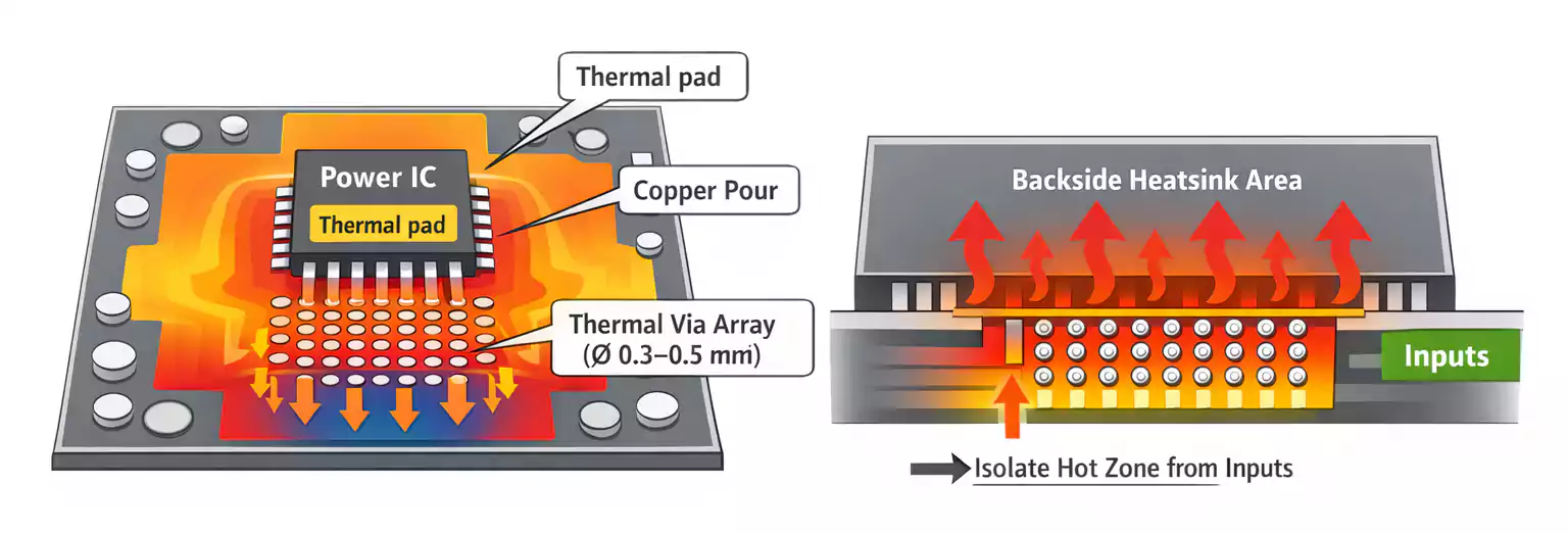
The Heat Path
Think of heat like current—it needs a low-resistance path to escape:
Chip → Pad → Copper Area → Thermal Vias → Heatsink or Board Backside
Design Tips
- Increase the copper area around transistors or ICs.
- Use arrays of thermal vias (0.3–0.5 mm) to connect the top and bottom copper layers.
- Avoid placing sensitive parts near hot devices.
- Simulate or measure temperature rise during prototyping.
Good thermal spreading can lower device temperature by 10–20°C, greatly extending component life.
Application-Specific Design Notes
1. Audio Power Amplifiers (Class-AB, Bridge, Single-Ended)
Audio circuits are very sensitive to hum and noise.
- Keep the signal ground and power ground separate, connecting them at a single point near the power input.
- Use twisted-pair or shielded input cables.
- Route speaker output lines away from input traces.
- Add a relay or muting circuit at startup to avoid the “pop” sound in speakers.
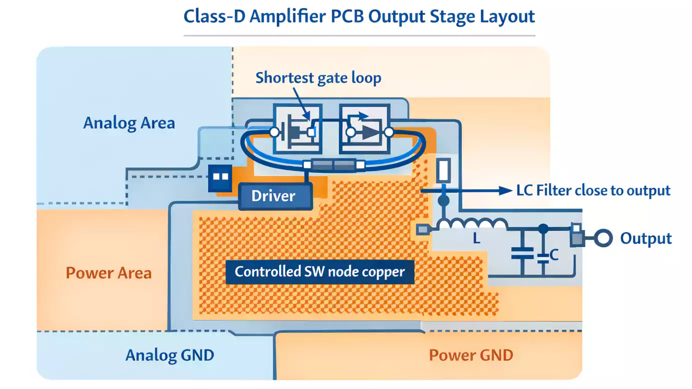
2. Class-D Switching Amplifiers
Class-D amplifiers switch at hundreds of kilohertz, so layout is critical.
- Keep the MOSFET gate loop as short as possible.
- The switching node (SW) should have minimal copper area to reduce EMI, but enough to handle heat.
- Place the LC output filters close to the output pins.
- Separate the analog input ground from the power stage ground.
3. Low-Noise Op-Amp or Instrumentation Amplifiers
For sensor and precision circuits:
- Keep feedback resistors right next to the op-amp pins.
- Route inputs symmetrically to reduce offset and noise.
- Add guard traces or ground shields around very high-impedance nodes.
- Control bandwidth with a small capacitor across the feedback resistor to improve stability.
PCB Pedal (Guitar Effects) Tips
Many musicians build or buy pcb pedal circuits to create custom guitar effects. Although these are smaller and lower-power than audio amplifiers, layout rules still apply.
- Use the metal enclosure as a common ground reference—it acts as a natural shield.
- Wire the footswitch carefully: avoid long, unshielded signal wires, as they can pick up hum.
- Implement True Bypass switching so the guitar signal passes cleanly when the effect is off.
- Place input and output jacks close to their circuit sections to keep traces short.
- If you use LEDs or digital control, isolate their ground paths to prevent noise coupling into the audio path.
A neat, well-grounded pedal PCB not only sounds better but is also easier to assemble and repair.
Final Thoughts
Designing a reliable and low-noise amplifier PCB circuit is both an art and a science.
By focusing on short signal paths, solid grounding, proper decoupling, and careful heat management, you can achieve professional-grade performance even in small DIY or high-volume applications.
Whether you are building an audio amplifier, a precision op-amp circuit, or a guitar pedal PCB, these layout rules apply everywhere.
At FastTurnPCB, we specialize in fast and high-quality PCB fabrication for amplifier projects of all kinds—from prototypes to mass production. With advanced equipment and strict quality control, we help engineers and hobbyists bring their amplifier designs to life quickly and reliably.
