In 5G systems, the RF front-end (RFFE) is the section that manages radio signals between the transceiver and the antenna. It typically includes power amplifiers, low-noise amplifiers, switches, filters, and matching networks that support signal transmission, reception, and band control.
Because these signals pass through high-frequency paths, the PCB is not just a mechanical carrier. Its material directly affects impedance control, insertion loss, conductor loss, thermal stability, and overall RF consistency.
That is why PCB material selection is critical to board-level 5G RF technology, especially in sub-6 GHz and mmWave applications. The right laminate is not simply the lowest-loss option on paper. It is the one that best matches the operating band, critical RF paths, thermal demands, and manufacturing requirements.
What Is a 5G RF Front-End Board?
A 5G RF front-end board is the part of the system that supports and interconnects the radio components between the transceiver and the antenna.
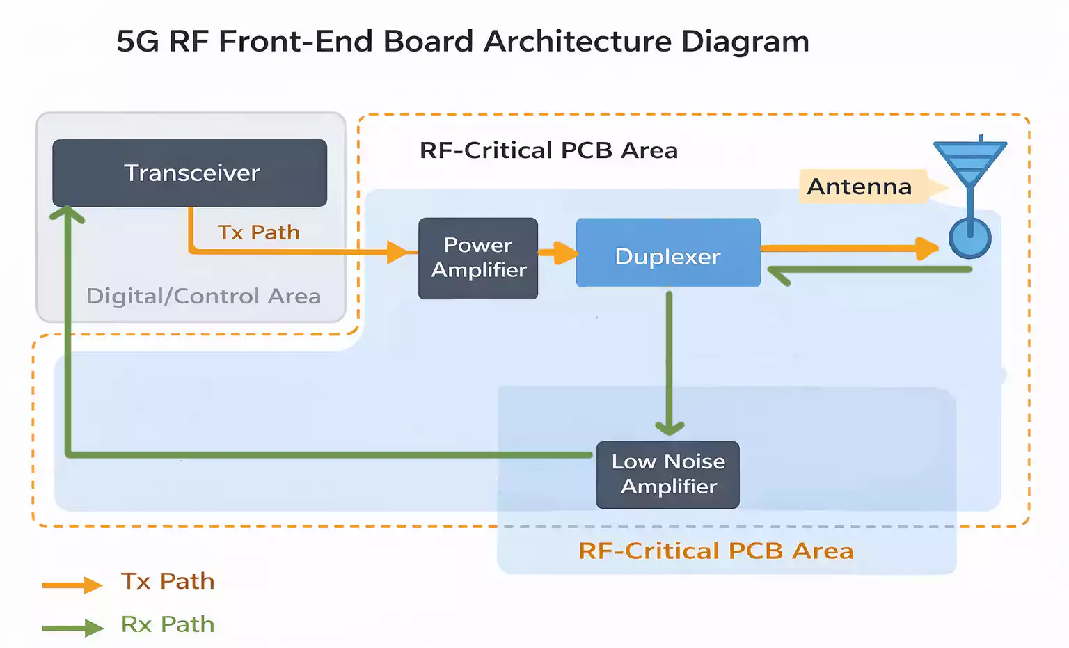
In practice, this is where many of the most sensitive RF design decisions are made.
Typical RF front-end building blocks include:
- Power amplifiers (PAs) for transmit power
- Low-noise amplifiers (LNAs) for weak received signals
- Filters for frequency selection and interference control, including each 5G RF filter used in the signal chain
- Switches for routing signals across bands and modes
- Duplexers for transmit/receive separation
- Matching networks for impedance continuity
- Antenna feed structures in more advanced designs
Because these functions operate at RF frequencies, the PCB does far more than hold components together. Trace geometry, dielectric thickness, ground reference quality, and material consistency all affect:
- insertion loss
- return loss
- coupling
- phase behavior
- thermal stability
In other words, the board itself becomes part of the circuit.
Why 5G Makes PCB Material Selection More Difficult
5G front-end design is more demanding than older narrowband RF designs for several reasons.
1. More bands mean more complexity
Many 5G products must support multiple 5G bands while maintaining compatibility with 4G and, in some cases, older standards.
That means:
- more filters
- more switches
- more routing congestion
- tighter component placement
- more front-end integration
2. More antennas mean tighter consistency requirements
5G systems often use more antennas and more parallel channels.
Even when the design is not a full mmWave phased-array module, MIMO architectures create stronger requirements for:
- path consistency
- channel-to-channel repeatability
- isolation
- phase stability
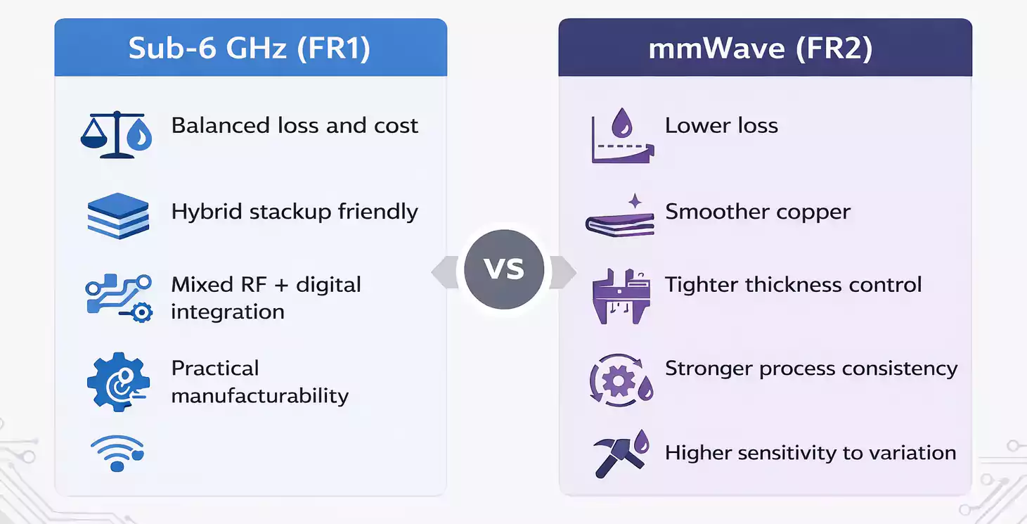
3. Sub-6 GHz and mmWave are not the same problem
One of the biggest mistakes in RF PCB material selection is treating all 5G boards the same.
They are not.
- Sub-6 GHz designs often balance RF performance with cost and mixed-signal integration.
- mmWave designs are far less forgiving. At higher frequencies, loss rises faster, and manufacturing variation becomes more visible.
4. Thermal density is higher
Power amplifier sections, compact RF modules, and dense routing create more heat in less space.
That means material selection must account for:
- heat spreading
- dimensional stability
- assembly reliability
- long-term performance consistency
The PCB Material Properties That Matter Most
When engineers talk about RF materials, they often focus first on Dk and Df.
Those are important, but they are not the whole story.
Dielectric Constant (Dk)
Dk affects:
- impedance
- propagation velocity
- wavelength on the PCB
- physical trace dimensions
In a 5G RF front-end board, stable Dk often matters as much as low Dk.
Why? Because Dk variation can shift:
- impedance
- phase response
- antenna feed behavior
- matching network performance
Dissipation Factor (Df)
Df affects dielectric loss.
Lower Df generally means lower signal attenuation, which becomes increasingly important in:
- long RF traces
- antenna feed lines
- high-frequency receive paths
- mmWave structures
Copper Roughness
This is one of the most overlooked RF material issues.
At higher frequencies, current flows near the conductor surface. Rough copper increases conductor loss, which can significantly impact real RF performance.
This becomes especially important in:
- mmWave front-end boards
- long feed networks
- low-loss receive paths
- high-efficiency transmit paths
Thickness Consistency
If the dielectric thickness varies, the impedance varies accordingly.
That affects:
- matching
- insertion loss
- repeatability
- multi-channel consistency
CTE and Dimensional Stability
Coefficient of thermal expansion matters because RF boards see thermal stress during:
- lamination
- solder reflow
- operation
- long-term temperature cycling
Poor dimensional stability can lead to:
- registration issues
- mechanical stress
- warpage
- long-term reliability risk
Thermal Conductivity and Heat Spreading
In PA areas, the board must help move heat away from critical components.
This affects:
- RF efficiency
- component reliability
- frequency stability
- product lifetime
Moisture Absorption
Moisture can shift dielectric properties and affect electrical consistency over time.
That matters more in:
- outdoor products
- infrastructure equipment
- temperature-variable environments
Sub-6 GHz vs mmWave: Different Material Priorities
Not every 5G board needs the same laminate strategy.
Sub-6 GHz material priorities
In many sub-6 GHz designs, the material decision is a balance between performance and cost.
Typical priorities include:
- acceptable insertion loss
- impedance stability
- manufacturability
- hybrid stackup compatibility
- mixed RF + digital integration
In some cases, premium RF material may only be needed on the most critical RF layers.
mmWave material priorities
mmWave boards demand much tighter control.
Typical priorities include:
- lower total loss
- more stable Dk
- smoother copper
- tighter thickness control
- stronger process consistency
At mmWave frequencies, even small variations can lead to significant performance shifts.
Quick comparison
| Loss sensitivity | Moderate to high | Very high |
| Copper roughness impact | Important | Critical |
| Thickness variation impact | Important | More severe |
| Cost pressure | High | High, but performance dominates |
| Hybrid stackup suitability | Often practical | Depends on design |
| Process tolerance sensitivity | Moderate | Very high |
Common Material Families for 5G RF Front-End Boards
There is no single best material family for every design.
FR4 and enhanced FR4
FR4 is still useful, but only in the right context.
It may work for:
- lower-frequency sections
- short RF paths
- digital control circuitry
- power management areas
- less sensitive support layers
It becomes risky when the board includes:
- long RF traces
- tighter loss budgets
- stronger phase consistency requirements
- mmWave operation
Low-loss hydrocarbon or ceramic-filled hydrocarbon laminates
These often provide a good balance between:
- RF performance
- manufacturability
- cost control
For many sub-6 GHz front-end applications, they are a practical middle ground.
PTFE-based laminates
PTFE-based materials are widely used for high-frequency RF applications due to their low-loss characteristics.
They can be an excellent choice for more demanding RF paths, but they also come with trade-offs:
- higher cost
- narrower fabrication window
- more process complexity
Ceramic-filled PTFE materials
These materials combine low loss with better dimensional and thermal stability.
They are often a strong fit for:
- higher-frequency RF paths
- more demanding 5G front-end designs
- cases where consistency matters as much as low loss
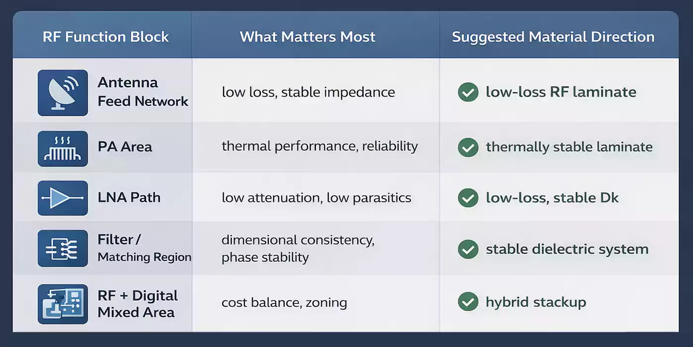
Choosing Material by RF Front-End Function Block
A smarter way to choose PCB material is by function block, not just by brand or generic material category.
For antenna feed networks
Priorities:
- low loss
- stable impedance
- good channel consistency
- controlled conductor loss
These paths usually benefit from improved dielectric stability and better control of the copper surface.
For power amplifier areas
Priorities:
- thermal performance
- heat spreading
- dimensional reliability
- acceptable RF behavior under load
In PA zones, thermal capability can matter just as much as electrical loss.
For low-noise receive paths
Priorities:
- low attenuation
- low parasitics
- controlled impedance
- cleaner signal preservation
Weak received signals should not lose unnecessary energy before reaching the active receive chain.
For filter and matching network regions
Priorities:
- stable Dk
- dimensional consistency
- predictable phase behavior
- repeatable electrical length
These structures are often sensitive to even small material variations. In particular, 5G RF filter performance can be affected by dielectric stability, conductor loss, and stackup consistency across the board.
For mixed RF + digital boards
Priorities:
- zoning
- stackup balance
- cost control
- targeted use of premium laminate
This is where hybrid stackups often make the most sense.
Can FR4 Still Be Used in 5G RF Front-End Boards?
Yes, but not blindly.
FR4 may still be acceptable when:
- The frequency is lower
- RF traces are short
- The loss budget is not extremely tight
- Critical RF paths are isolated to specific areas
- The board includes substantial digital/control circuitry
FR4 becomes risky when:
- RF traces are longer.
- insertion loss must be minimized
- Phase consistency matters across channels
- The design moves toward mmWave
- thermal and dimensional demands are higher
Best practical rule
Do not ask, “Can this whole board be FR4?”
Ask instead:
- Which paths are truly RF-critical?
- Which areas are digitally dominated?
- Where does premium laminate actually improve performance?
That question leads naturally to hybrid stackup decisions.
Why Hybrid Stackups Often Make Sense
For many 5G RF front-end boards, the most practical solution is neither an all-RF laminate stackup nor an all-FR4 stackup.
It is a hybrid approach.
A hybrid stackup can allow:
- RF-critical layers to use high-frequency material
- digital and control layers to remain on standard materials
- better cost control
- improved manufacturing realism
- more targeted performance improvement
This approach is especially useful in mixed RF + digital front-end boards where only part of the structure is highly loss-sensitive.
Common Mistakes to Avoid
Here are some of the most common material-selection mistakes in 5G RF front-end design:
1. Choosing material by Dk alone
A low Dk does not guarantee the best RF result.
2. Ignoring Df and copper roughness
Dielectric loss is only part of the total loss picture.
3. Treating sub-6 and mmWave the same
They have different electrical and manufacturing sensitivities.
4. Over-specifying premium laminate across the whole board
That raises cost without always improving the noncritical parts of the design.
5. Ignoring thermal and dimensional stability
Good electrical numbers alone do not ensure long-term reliability.
6. Selecting material before discussing fabrication limits
A realistic material strategy should always include the PCB manufacturer early.
A Practical Material Selection Workflow
A strong selection process usually follows this order:
Step 1: Define the operating band
Is the board sub-6 GHz, mmWave, or mixed?
Step 2: Identify the most loss-sensitive RF paths
Focus first on the traces and structures that most strongly affect RF performance.
Step 3: Set electrical targets
Define the real goals for:
- impedance
- insertion loss
- phase stability
- isolation
Step 4: Evaluate thermal and reliability needs
Consider heat, CTE, dimensional stability, and environment.
Step 5: Decide between full RF laminate and hybrid stackup
Do not assume one material must be used everywhere.
Step 6: Validate the stackup with fabrication capability
The best theoretical answer is not always the best production answer.
Final Thoughts
Selecting the right PCB material for a 5G RF front-end board is a design decision, not a default specification. The best choice depends on the actual RF path, operating band, thermal conditions, manufacturing limits, and cost targets.
For many sub-6 GHz designs, a balanced or hybrid stackup offers the most practical solution. For mmWave applications, lower-loss materials, smoother copper, and tighter process control usually become more important.
In the end, the best material is the one that supports RF performance where it matters most while remaining manufacturable and cost-effective—something that also depends on your high-frequency PCB manufacturer's capabilities.