

Introduction
A flying lead flex PCB is a special flexible circuit structure where a section of copper conductor is locally exposed for bonding, contact, or interconnection. This structure is often used in HDI flex PCBs, fine-pitch interconnects, compact electronic assemblies, and applications that require access to the conductor from one or both sides.
Unlike standard flex circuits, a flying lead area has limited dielectric support. This makes the copper conductor more vulnerable to bending, deformation, and breakage during fabrication, handling, and final use.
Because of this, the flying lead flex PCB manufacturing process requires careful control of circuit design, routing, coverlay opening, lamination alignment, dimensional stability, and adhesive flow.
Quick Answer
The flying lead flex PCB manufacturing process is challenging because the exposed copper conductor has little or no dielectric support.
Traditional pre-cut coverlay processes can be used for larger openings, but they become less reliable for smaller openings. When the opening is below 1.0 mm, dimensional accuracy, adhesive squeeze-out, and process yield become difficult to control.
For high-density designs, advanced processes such as laser ablation, plasma etching, and chemical etching are often used to achieve better precision and manufacturing stability.
Why Flying Lead Flex PCBs Are Difficult to Manufacture
The main challenge of a flying lead structure comes from the unsupported copper conductor.
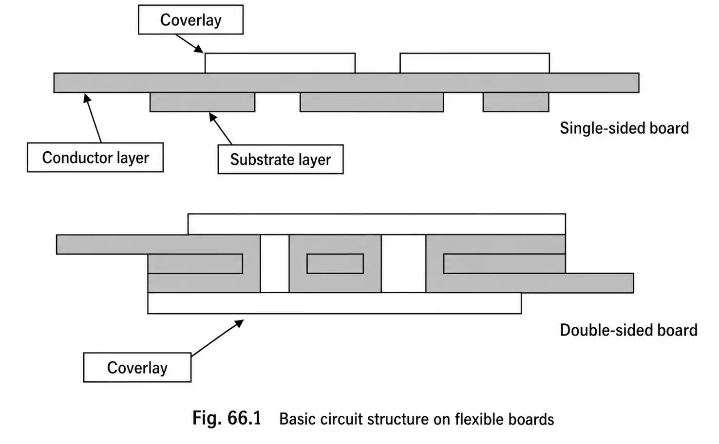
In a standard flex PCB, copper traces are protected by the base film and coverlay. In a flying lead area, part of the coverlay or dielectric material is selectively removed to expose the copper.
This creates several manufacturing risks:
- The flying lead area can bend easily.
- Fine copper conductors may deform or break.
- Coverlay window alignment becomes more difficult.
- Small openings are harder to control dimensionally.
- Adhesive may flow into the window area.
- HDI fine-line structures may have lower production yield.
- Rework and scrap costs may increase.
For this reason, flying lead design should be considered early in the PCB design stage. Trace width, coverlay window size, support area, and process capability all affect manufacturability.
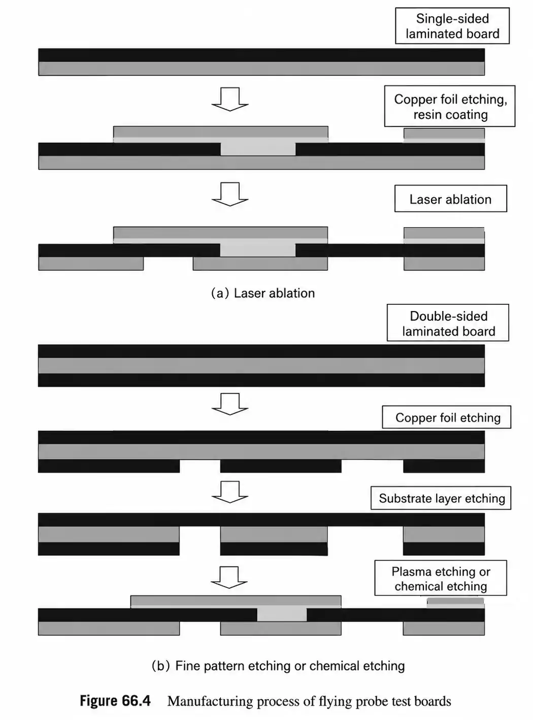
Traditional Flying Lead Flex PCB Manufacturing Process
A common flying lead structure is made using a pre-cut coverlay process. In this method, the coverlay is opened before lamination, then laminated with copper foil to form the required exposed conductor area.
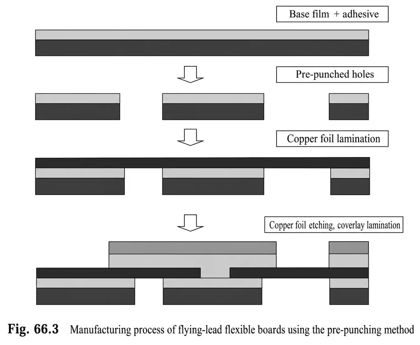
1. Pre-Cut the Coverlay Window
The first step is to create an opening in the coverlay.
Common methods include:
- Laser cutting
- Die punching
- Mechanical drilling
This opening defines the area where the copper conductor will later be exposed.
2. Laminate the Coverlay to Copper Foil
After the coverlay window is prepared, it is laminated to the matte side of the copper foil.
The copper foil is usually prepared with registration holes. These holes help align the coverlay opening with the future circuit pattern.
Accurate registration is critical. Poor alignment may lead to:
- Insufficient conductor exposure
- Offset window position
- Damaged flying lead areas
- Reduced process yield
3. Apply Dry Film or Wet Film
After lamination, dry film or wet film is applied to the panel.
This step prepares the copper surface for image transfer and circuit etching.
4. Etch the Circuit Pattern
The copper circuit is then formed through etching.
For flying lead structures, trace integrity is especially important. Since part of the copper conductor will later be unsupported, uneven etching, narrow trace width, or stress concentration can increase the risk of conductor breakage.
5. Laminate the Second Pre-Cut Coverlay
After the circuit is etched, a second pre-cut coverlay is laminated on the top side of the circuit.
When the openings on both sides are aligned, the selected copper section remains exposed, forming the flying lead structure.
Limitations of the Pre-Cut Coverlay Process
Although the pre-cut coverlay process is widely used, it has several limitations for HDI flex PCB flying lead structures.
Complex Workflow
The process includes coverlay cutting, copper foil registration, lamination, film application, circuit etching, and second-side coverlay lamination.
This increases labor, equipment usage, material consumption, and process control requirements.
Low Production Flexibility
Since the coverlay opening is prepared before lamination, any change in the circuit layout, window size, or flying lead position may require process adjustments.
This is not ideal for small-batch production, multiple product versions, or designs that change frequently.
Lower Production Efficiency
Multiple alignment and lamination steps slow down production.
For HDI fine-line structures, each additional process step can introduce variation and reduce final yield.
Poor Coverlay Dimensional Stability
Coverlay is flexible by nature. After pre-cutting, its dimensional stability becomes harder to control.
The connection area and window area are especially sensitive to deformation, movement, and size variation.
Higher Risk of Thin Copper Foil Damage
HDI flex PCBs often use thin copper foil.
During pre-cutting, lamination, and handling, thin copper is more vulnerable to stretching, wrinkling, scratching, or breaking.
Difficult Yield Control for Small Windows
When the opening becomes smaller, the traditional process becomes much harder to control.
For openings below 1.0 mm, it is difficult to maintain:
- Accurate window size
- Stable coverlay alignment
- Controlled adhesive flow
- Consistent conductor exposure
- Stable production yield
Adhesive Squeeze-Out in Flex PCB Coverlay Openings
Adhesive squeeze-out is one of the most important issues in the flying lead flex PCB manufacturing process.
Coverlay usually includes an adhesive layer. During lamination, heat and pressure cause the adhesive to flow. If the window is very small, the adhesive may flow into the opening.
This can cause:
- Reduced exposed copper area
- Uneven window edges
- Poor bonding, soldering, or connection performance
- Contamination of fine-line areas
- Lower product consistency
For openings smaller than 1.0 mm, relying only on traditional pre-cut coverlay is often not enough to achieve stable window quality.
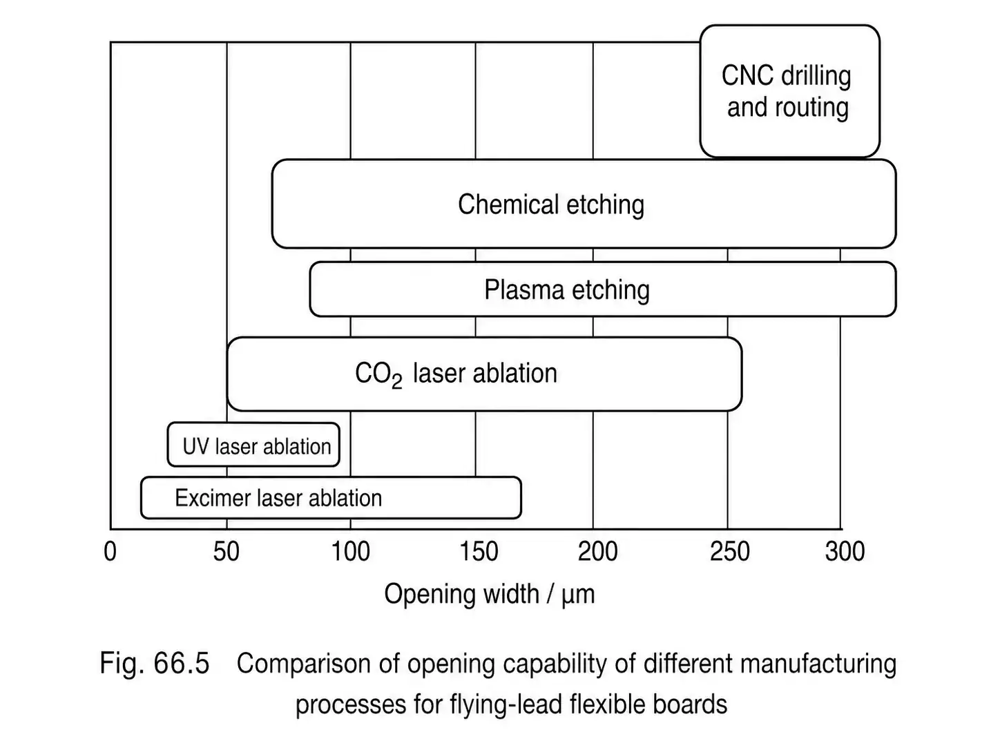
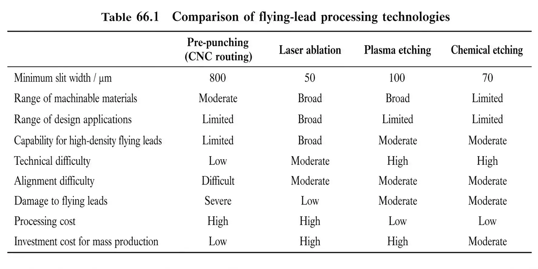
High-Precision Opening Technologies for Flying Lead Flex PCBs
To meet the precision requirements of HDI flex PCBs, manufacturers often employ advanced selective material-removal processes.
The most common options are:
- Laser ablation
- Plasma etching
- Chemical etching
Process Comparison
| Process | Main Advantage | Limitation | Best Used For |
| Pre-cut coverlay | Simple and widely used | Limited precision for small windows | Larger openings and simpler structures |
| Laser ablation | High precision and flexible pattern control | Requires careful laser parameter control | Small windows, local openings, HDI routing areas |
| Plasma etching | Low mechanical stress on flex materials | Process speed and material selectivity need control | Thin copper and stress-sensitive structures |
| Chemical etching | Good dimensional control for suitable materials | Requires tight chemistry and compatibility control | Precision material removal and stable production windows |
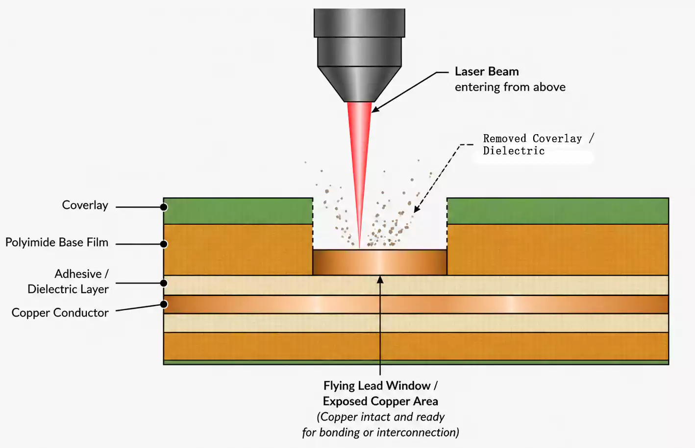
Laser Ablation for Flex PCB Flying Leads
Laser ablation for flex PCB manufacturing uses focused laser energy to selectively remove coverlay or dielectric material.
Compared with mechanical punching, laser processing can reduce material deformation and improve control over window position and shape.
Laser ablation is especially suitable for:
- Fine openings
- Localized material removal
- Complex window shapes
- HDI flex PCB flying lead areas
- High-density routing regions
Plasma Etching for HDI Flex PCB
Plasma etching for HDI flex PCB removes material through a plasma-based reaction.
Because it does not rely on mechanical cutting, it creates less mechanical stress on flexible materials. This helps reduce the risk of damaging thin copper foil or delicate flex structures.
Plasma etching is useful when the design requires fine material removal with lower mechanical impact.
Chemical Etching for Flexible PCB Openings
Chemical etching for flexible PCB openings removes material through a controlled chemical reaction.
It can be used for high-precision openings or localized material removal in some flying lead structures.
However, chemical etching requires careful control of:
- Chemistry
- Material compatibility
- Etching uniformity
- Process stability
The final choice depends on the material system and required tolerance.
How to Choose the Right Flying Lead Manufacturing Process
There is no single process that works for every flying lead flex PCB design.
The right choice depends on several factors:
- Window size
- Flying lead length
- Trace width and spacing
- Copper foil thickness
- Coverlay material
- Alignment tolerance
- HDI fine-line requirements
- Final connection method
- Production efficiency
- Cost and yield targets
For larger openings and simpler structures, traditional pre-cut coverlay may still be practical.
For small windows, fine-line routing, or HDI flex PCB flying lead structures, laser ablation, plasma etching, or chemical etching usually provides better precision and process stability.
Key Takeaways
Flying lead structures provide useful interconnection options for HDI flex PCBs, but they are challenging to manufacture.
The biggest issue is the lack of dielectric support around the exposed copper conductor. This makes the flying lead area more sensitive to bending, deformation, and breakage.
Traditional pre-cut coverlay can work for basic structures, but it has limitations in small-window accuracy, adhesive control, dimensional stability, production efficiency, and yield.
When the opening is smaller than 1.0 mm, high-precision processes such as laser ablation, plasma etching, and chemical etching are often better suited for stable manufacturing.
Conclusion
Flying lead manufacturing requires more than simply opening the coverlay. It depends on accurate design, stable materials, precise alignment, and the right material removal process.
For HDI flex PCBs, especially designs with small windows and fine-line routing, choosing the right process is critical to improving yield, reducing cost, and maintaining reliable conductor performance.
FastTurnPCB supports custom flex and rigid-flex PCB manufacturing, including high-density designs that require precise coverlay openings and controlled flying lead structures.
