

A flying lead flex PCB is a special flexible circuit structure that allows a copper conductor to be accessed from both sides. This is achieved by selectively removing the coverlay on one side and the base film on the opposite side, leaving the copper conductor locally exposed.
Because flexible PCBs use very thin dielectric materials, they can support structures that are difficult to manufacture with traditional rigid PCBs. The flying-lead structure is one example. It is widely used in high-density flexible circuits, TAB bonding, chip-scale packaging, hard disk drive suspension assemblies, ultrasound probes, and other compact electronic applications.
Quick Answer: What Is a Flying Lead Flex PCB?
A flying lead flex PCB is a flexible printed circuit in which a single copper conductor is exposed from both sides.
In a standard flex circuit, one side of the copper may be covered by coverlay, while the other side is supported by the base film. In a flying-lead structure, both insulating layers are removed in a defined area. This allows the same copper conductor to be contacted, bonded, or connected from either side.
This type of structure is also closely related to terms such as:
- Flying Lead Flexible PCB
- Flying Lead FPC
- Dual Access Flex PCB
- Back-bared Flex Circuit
- TAB Flying Lead
Why Flexible PCBs Can Support Flying-Lead Structures
Flexible PCBs are built with thin and flexible dielectric materials, such as polyimide. Compared with rigid PCB materials, these thin films are easier to process locally.
This allows manufacturers to create special structures by using processes such as:
- coverlay opening
- base film removal
- window creation
- selective dielectric removal
- localized copper exposure
These features make flexible PCBs suitable for compact, lightweight, and high-density interconnect designs.
A flying lead flex PCB takes advantage of this material flexibility by exposing the same copper conductor from both sides in a controlled area.
Basic Structure of a Flying Lead Flex PCB
A typical flying-lead structure includes the following parts:
| Copper conductor | Provides the electrical path and contact area |
| Base film | Supports the copper in the normal flex area |
| Coverlay | Protects and insulates the conductor |
| Flying-lead area | Exposes the copper from both sides |
| Surrounding support area | Keeps the conductor mechanically stable |
The most important feature is that the copper conductor remains part of the flex circuit, but the surrounding organic insulating material is removed in the flying-lead area.
This creates a local section of exposed copper that can be used for bonding, contact, or special interconnection.
How a Flying-Lead Structure Works
The working principle of a flying lead flex PCB is simple, but the manufacturing process must be very precise.
1. Start with a fine-pitch copper conductor
Flying leads are usually made from a single layer of fine-pitch copper conductors. This copper layer is laminated onto a thin, flexible base material.
2. Open the coverlay
The coverlay is removed in the target area to expose one side of the copper conductor.
3. Remove the base film on the opposite side
The base film is then selectively removed from the same location on the opposite side.
After these steps, the copper conductor is exposed from both sides, while the surrounding flexible circuit structure continues to provide support.
Flying Leads in Single-Sided Flexible PCBs
In a single-sided flexible PCB, the copper foil is usually located between the base film and the coverlay.
Under normal conditions:
- The coverlay side can be opened to expose the copper.
- The base-film side remains insulated.
- The copper conductor is supported by the surrounding dielectric material.
To create a flying-lead structure, both sides of the target conductor area must be processed.
| Coverlay opening | Exposes one side of the copper |
| Base film removal | Exposes the opposite side of the copper |
| Surrounding dielectric area | Provides mechanical support |
This allows one copper layer to provide two-sided contact in a local area.
Single-sided flying-lead flexible PCBs are often used for fine-pitch bonding, chip-to-chip connections, lightweight assemblies, and high-density interconnect applications.
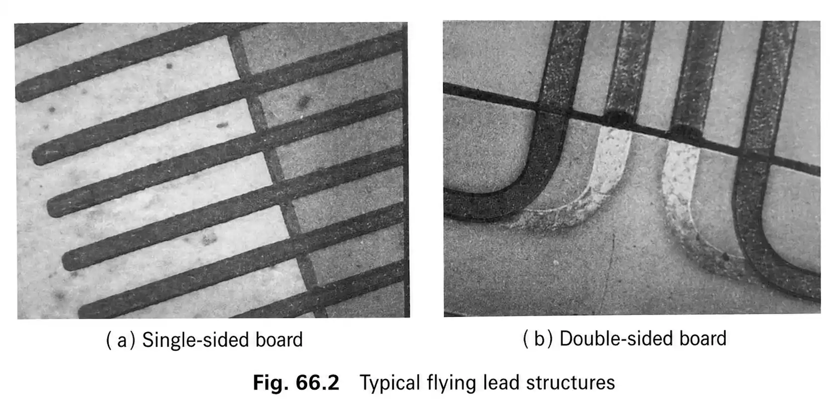
Flying Leads in Double-Sided Flexible PCBs
Flying-lead structures can also be used in double-sided flexible PCBs, but the design is more complex.
A double-sided flex PCB has copper on both sides of the base film. To create a flying-lead area, the manufacturer must carefully define:
- Which copper area remains exposed
- Which dielectric material is removed
- where the coverlay openings are placed
- How much support remains around the conductor
Compared with single-sided flying leads, double-sided flying-lead structures can support more complex interconnect requirements. However, they also require tighter process control.
If the opening position, conductor width, or dielectric removal area is poorly controlled, the flying-lead area may suffer from deformation, poor contact, or reliability issues.
Flying Lead Flex PCB vs. Standard Double-Sided Interconnection
A flying lead flex PCB is sometimes confused with a standard double-sided PCB connection. However, the two structures are different.
| Main purpose | Exposes one conductor from both sides | Connects two copper layers |
| Typical method | Local coverlay and base film removal | Vias or plated through holes |
| Copper structure | Same conductor accessible from both sides | Different layers connected together |
| Key benefit | Direct contact or bonding access | Conventional layer-to-layer connection |
| Typical use | TAB bonding, HDI flex, chip packaging | Standard PCB routing |
The key point is:
A flying lead flex PCB is not mainly about connecting two copper layers. It is about making the same copper conductor accessible from both sides.
Common Applications of Flying Lead Flexible PCBs
Flying lead flexible PCBs are used in applications that require fine-pitch connections, compact structures, and reliable two-sided conductor access.
| HDI flexible circuits | Support fine-pitch and high-density interconnects |
| Hard disk drive suspension assemblies | Provide lightweight and precise electrical connections |
| Chip-scale package interposers | Enable compact chip-to-package connections |
| Ultrasound probes | Support dense signal paths in limited space |
| TAB bonding | Provides exposed fine-pitch conductors for chip bonding |
| Compact electronic modules | Reduces space and supports special contact methods |
Among these applications, the TAB flying lead is one of the most important use cases. TAB requires accurate fine-pitch conductors, stable bonding areas, and reliable electrical contact. A flying-lead structure provides a thin, precise conductor that can be accessed from both sides.
Why Flying Leads Are Useful in HDI Flex Circuits
HDI flex circuits require fine lines, tight spacing, compact routing, and reliable interconnection. A flying lead flex PCB is well-suited for these requirements because it allows high-density copper conductors to be exposed in very small areas.
The main advantages include:
Thinner local structure
Because part of the coverlay and base film is removed, the flying-lead area can be thinner than the surrounding flex circuit.
Two-sided conductor access
The same copper conductor can be contacted from either side. This is useful for bonding, assembly, packaging, and special contact methods.
Fine-pitch capability
Flying leads can be combined with fine-line routing and precise openings, making them suitable for HDI flexible PCB designs.
Compact interconnection
In some applications, flying leads can reduce the need for bulky connectors or conventional interconnection methods.
Manufacturing Challenges of Flying Lead Flex PCBs
Although flying-lead structures provide important design advantages, they are difficult to manufacture.
The process requires accurate control of:
- coverlay opening
- base film removal
- copper protection
- conductor alignment
- dimensional stability
- production yield
Traditional methods, such as pre-punching and pre-drilling, can be used to remove material in selected areas. However, these methods may not be ideal for advanced fine-pitch or high-volume production.
| Limited processing accuracy | Misalignment in fine-pitch areas |
| Inconsistent material removal | Uneven copper exposure |
| Weak local support | Copper deformation or cracking |
| Lower process yield | Higher production cost |
| Poor dimensional control | Reduced assembly reliability |
To expand the use of flying-lead FPC structures, manufacturers need processes that support higher precision, greater consistency, and lower cost.
Key Design Considerations for Flying Lead FPC
Designing a flying lead FPC is not simply a matter of exposing copper. The structure must balance electrical access, mechanical support, manufacturability, and reliability.
Important design factors include:
- flying-lead location
- exposed conductor length
- conductor width and spacing
- coverlay opening size
- base film removal size
- alignment between both openings
- remaining support around the conductor
- surface finish on exposed copper
- bonding or contact method
- manufacturing tolerance capability
Because the flying-lead conductor is partially unsupported, poor design may lead to bending, cracking, deformation, or unstable contact.
The surrounding structure must provide sufficient support while still allowing access to the copper from both sides.
Benefits and Limitations of Flying Lead Flex PCB
Benefits
A flying lead flex PCB offers several important advantages:
- enables two-sided conductor contact
- supports fine-pitch interconnection
- reduces local structure thickness
- works well in compact electronic assemblies
- supports TAB and advanced packaging applications
- can be used in HDI flexible circuits
Limitations
However, this structure also has limitations:
- more difficult to manufacture
- requires precise material removal
- provides less local mechanical support
- may increase cost if the yield is low
- requires careful design and process control
For this reason, flying-lead structures are not necessary for every flexible PCB. They are best used when a standard single-sided, double-sided, or rigid-flex PCB cannot meet the connection requirements.
When Should You Use a Flying Lead Flex PCB?
A flying lead flex PCB may be a good choice when your design requires:
- direct access to the same copper conductor from both sides
- fine-pitch bonding
- compact chip or module interconnection
- reduced local thickness
- high-density flexible routing
- TAB bonding or similar packaging methods
- special contact or assembly requirements
However, if the design only requires standard routing or a standard layer-to-layer connection, a conventional flexible PCB or a rigid-flex PCB may be more practical and cost-effective.
FAQ About Flying Lead Flex PCB
What is a flying lead flex PCB?
A flying lead flex PCB is a flexible circuit structure in which a single copper conductor is exposed from both sides by removing the coverlay and base film in a defined area.
Is a flying lead flex PCB the same as a double-sided flex PCB?
No. A double-sided flex PCB usually has copper on both sides of the base film. A flying-lead structure exposes the same copper conductor from both sides for direct contact or bonding.
Where are flying lead flexible PCBs used?
Flying lead flexible PCBs are commonly used in HDI flex circuits, TAB bonding, hard disk drive suspension assemblies, chip-scale package interposers, ultrasound probes, and compact electronic modules.
Why is the flying-lead structure difficult to manufacture?
It requires precise coverlay opening, base film removal, copper protection, alignment control, and mechanical support. Poor process control can lead to deformation, cracking, or low yield.
What is the main advantage of a flying-lead structure?
The main advantage is two-sided access to the same copper conductor. This makes it useful for fine-pitch bonding, compact packaging, and high-density flexible interconnects.
Conclusion
A flying lead flex PCB exposes a single copper conductor from both sides by selectively removing the coverlay and base film in the same area. This creates a precise contact section that can be bonded, contacted, or connected from either side.
This structure is especially useful in HDI flex circuits, TAB bonding, chip-scale packaging, ultrasound probes, hard drive suspension assemblies, and compact electronic modules where fine pitch, low profile, and reliable interconnection are critical.
Because the exposed conductor has limited mechanical support, successful implementation depends on accurate material removal, proper conductor support, tight alignment, and stable process control.
For designs that require compact, high-density, two-sided conductor access, FastTurnPCB can support flexible PCB solutions from design review to manufacturing.
