Decoupling capacitors should be placed as close as possible to the IC power pins to minimize parasitic inductance and keep the high-frequency current loop small. In high-frequency PCB design, even a good capacitor may perform poorly when connected via long traces, distant vias, or a weak return path.
That is why effective placement of decoupled capacitors is not only about capacitor value. Placement, via location, loop area, and return path quality, often has a greater impact on real board performance.
Poor decoupled capacitor layout can lead to EMI problems, unstable clocks, ADC noise, power rail ringing, and degraded RF behavior. This article explains where decoupling capacitors should be placed, which layout mistakes matter most, and how to improve decoupling performance in high-frequency PCB design.
Key Takeaways
- Place the decoupled capacitor as close as possible to the IC power pin.
- Focus on minimizing loop inductance, not just physical distance.
- Keep the connection between the pin, capacitor, and ground return short and direct.
- A solid ground plane greatly improves decoupled capacitor performance.
- One capacitor value is usually not enough for the full frequency range.
- In high-frequency designs, layout quality often matters more than nominal capacitance.
What Is a Decoupling Capacitor in PCB Design?
A decoupling capacitor is a capacitor placed between a power rail and ground near an active device to support fast local current demand and reduce voltage fluctuation on the supply line.
When an IC switches, it may draw current much faster than the wider power distribution network can respond. The decoupling capacitor acts as a local energy source, helping keep the voltage at the power pin stable during the transient event.
At the same time, it provides a low-impedance path for high-frequency noise, helping keep it local rather than letting it spread across the PCB.
Decoupling capacitor vs. bypass capacitor
In practice, the terms decoupling capacitor and bypass capacitor are often used interchangeably.
There is a slight difference in emphasis:
| Decoupling capacitor | Isolates one circuit block from disturbances caused by another |
| Bypass capacitor | Routes unwanted AC noise from power to ground |
In a real PCB layout, the same capacitor often serves both functions.
Why Decoupling Matters More in High-Frequency PCB Design
At low speed, a board can sometimes tolerate less-than-ideal capacitor placement.
At high frequency, it usually cannot.
That is because high-frequency behavior is heavily affected by parasitic inductance. Even if the capacitor value looks correct on paper, the actual connection path may add enough inductance to make the capacitor ineffective where it is needed most.
What really limits high-frequency decoupling?
At high frequency, performance is shaped by more than capacitance:
- ESL (equivalent series inductance)
- ESR (equivalent series resistance)
- trace inductance
- via inductance
- pad geometry
- return path quality
The real goal is not to “add more capacitance.” It is to keep PDN impedance low across the frequencies that matter.
Why Poor Decoupling Causes Real PCB Problems
Poor decoupling does not always show up as an obvious power issue. It can appear in several ways across the system.
Common symptoms of poor decoupling
- random resets or brownout events
- noisy ADC readings
- clock instability or jitter
- elevated EMI emissions
- transient ringing on power rails
- ground bounce
- degraded RF gain or receiver sensitivity
- inconsistent behavior across temperature or load
A board may look electrically correct in the schematic and still fail in the lab because the decoupling path is not physically optimized in layout.
Where to Place Decoupling Capacitors on a PCB
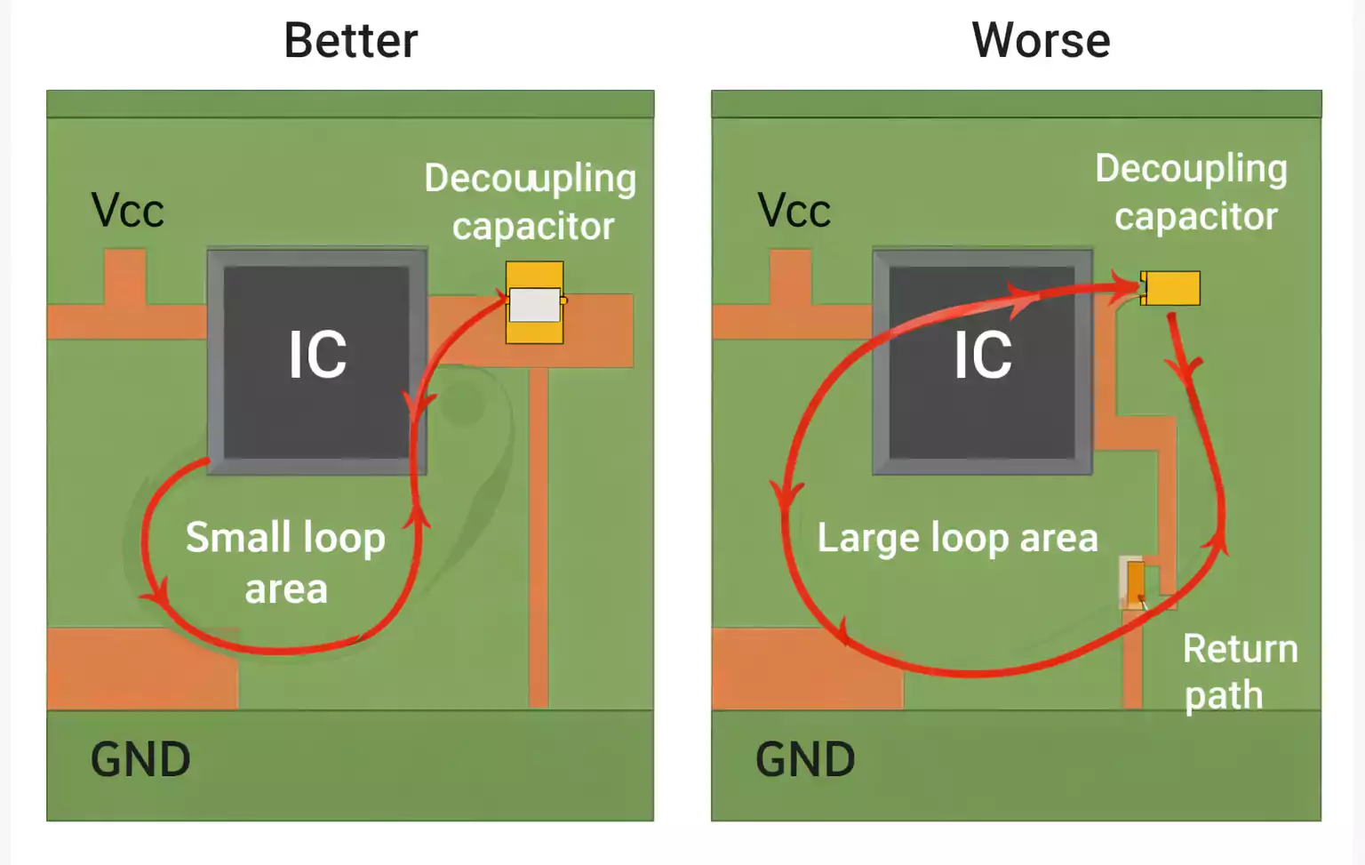
The basic rule is simple: place the decoupling capacitor as close as possible to the IC power pin.
In high-frequency PCB layout, however, “close” does not just mean physically nearby. It means the entire current path between the power pin, the capacitor, and the return path is short and low inductance.
That loop typically includes:
- The IC power pin
- the decoupling capacitor
- the ground or return path
- the associated vias and planes
What matters most
| Short path from pin to capacitor | Reduces inductance |
| Short path from capacitor to return path | Improves high-frequency current return |
| Small loop area | Reduces EMI and improves transient response |
| Closely spaced power and ground vias | Keeps the loop compact |
Best placement principle
Do not judge placement by appearance alone.
The real goal is to create the smallest possible current loop.

Minimize Loop Inductance, Not Just Distance
A capacitor can look close to the IC and still perform poorly.
That happens when:
- The routing path is long.
- The ground via is far away.
- The power and ground vias are separated.
- The capacitor is connected through narrow or indirect traces.
In high-frequency PCB design, loop inductance is often more important than straight-line distance.
Bad approach
- The capacitor appears near the IC.
- long trace runs from the power pin to the capacitor
- separate the ground by placing it farther away
Better approach
- The power pin connects directly to the capacitor.
- The capacitor connects directly to a nearby return path.
- Power and ground vias are kept close together.
Avoid Long Traces Between the Pin, Capacitor, and Via
Long or narrow traces add inductance. That makes the decoupling path less effective at high frequency.
Even when board space is tight, try to avoid:
- long trace stubs
- meandering routes
- thin neck-downs in the decoupling path
- extra bends between the pin and the capacitor
- unnecessary routing between the capacitor pad and the via
Practical rule
Use the shortest and most direct connection possible between:
- The IC power pin
- the decoupling capacitor
- the return path
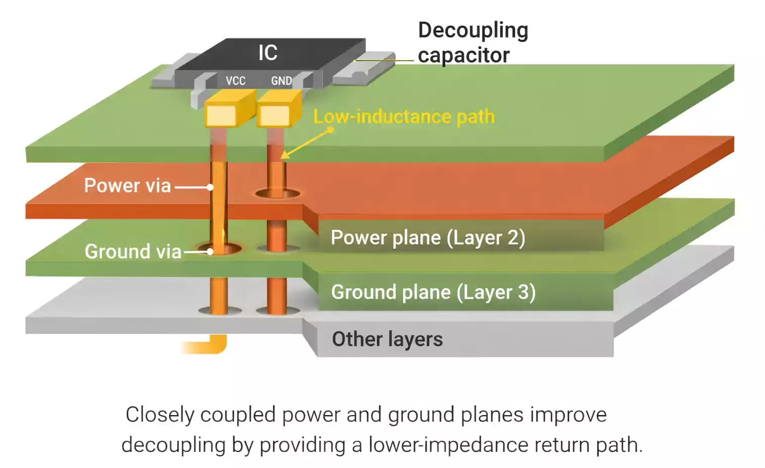
Keep Power and Ground Vias Close Together
Power and ground via spacing directly affects loop inductance.
If the two vias are placed too far apart, the current loop becomes larger. That increases inductance and weakens high-frequency decoupling.
Why via spacing matters
| Via placement | Effect |
|---|---|
| Power and ground vias close together | Smaller loop area and better high-frequency performance |
| Power and ground vias far apart | Larger loop area, higher inductance, and weaker decoupling |
This becomes even more important when the capacitor connects into internal planes rather than staying on surface routing..
How Far Should Decoupling Capacitors Be?
There is no universal rule for the distance between decoupling capacitors. The best practice is still to place them as close as possible to the IC power pin while keeping the current loop short and low inductance.
The acceptable distance depends on several factors, including edge rate, frequency content, stackup, package type, plane spacing, and return path quality.
When distance matters more
Placement becomes more critical when:
- The board does not have a solid power or ground plane
- Power and ground planes are widely spaced
- The connection path requires multiple vias
- Switching edges is very fast
When placement is slightly more forgiving
Placement can be somewhat less critical when:
- Power and ground planes are closely spaced
- The return path is strong and continuous
- The connection to the plane has low inductance
Even in these cases, closer placement is still preferred.
Do Decoupling Capacitors Need a Ground Plane?
Not strictly, but a ground plane makes them far more effective.
A solid ground plane provides a continuous, low-impedance path for high-frequency return current. That improves both decoupling performance and EMI behavior.
Ground plane vs. no ground plane
| Solid ground plane | Better return path, lower impedance, more predictable behavior |
| No ground plane | Works, but becomes more sensitive to routing inductance and loop area |
On boards without a ground plane
You should still:
- place local decoupling near every active device
- keep loops small
- Provide bulk support for each rail.
- keep power and return paths compact
Without a good plan, layout discipline matters even more.
How to Choose Decoupled Capacitor Value, Size, and Voltage Rating
Good decoupling requires the right capacitor network, not just a familiar default value.
Decoupling capacitor value vs. frequency
Smaller capacitors usually work better at higher frequencies because they often have lower inductance and higher self-resonant frequency.
Larger capacitors store more energy and help with slower current transients.
That is why designers often combine values.
Common capacitor roles
| Small ceramic capacitor | Very high frequency local decoupling |
| Mid-value capacitor | Intermediate transient support |
| Bulk capacitor | Lower frequency rail stabilization |
Typical value ranges
These are common starting points, not universal rules:
- 0.01 µF to 0.1 µF for local high-frequency decoupling
- 1 µF to 10 µF or more for broader transient or bulk support
Always check the IC datasheet for rail-specific guidance.
Why package size matters
Smaller packages usually have lower parasitic inductance.
That is why 0201, 0402, and 0603 packages are often preferred for high-frequency decoupling. However, package choice also depends on:
- manufacturing capability
- assembly reliability
- rework strategy
- board density
Voltage rating
Choose a voltage rating that is safely above the operating voltage, and remember that ceramic capacitors may lose effective capacitance under DC bias.
Should You Use One Capacitor or Multiple Capacitors?
In most high-frequency PCB designs, one capacitor is not enough.
That is because power noise and transient demand typically span multiple frequency ranges.
Why do multiple capacitors help
Different capacitors perform best at different frequency ranges. Using more than one helps keep PDN impedance lower across a wider bandwidth.
Common strategy
- One small capacitor very close to the power pin
- one or more additional capacitors for mid-range support
- One bulk capacitor farther upstream on the rail
Important note
More capacitors do not automatically mean better performance.
If they are poorly placed or connected, or chosen without considering resonance and package parasitics, they may provide little benefit.
Placement Strategies for Different PCB Power Plane Configurations
The best decoupling strategy depends partly on how the board distributes power.
1. Boards without power planes
These boards rely more heavily on local discrete capacitors.
Best practices:
- Place at least one local decoupling capacitor per active device.
- Provide at least one bulk capacitor per rail.
- minimize loop area aggressively
2. Boards with closely spaced power planes
These boards can support high-frequency power delivery more effectively because the plane structure itself helps.
Best practices:
- keep entry into the planes low inductance
- Place local capacitors near the IC region.
- maintain a strong return path
3. Boards with widely spaced power planes
These boards get less benefit from plane capacitance.
Best practices:
- Place capacitors closer to the IC
- avoid long vertical or horizontal decoupling paths
- Prioritize compact same-side placement where possible.
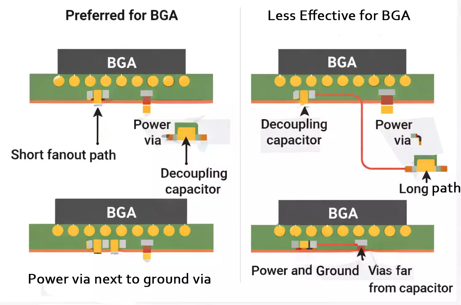
BGA and High-Density Layout Guidelines
BGAs create special decoupling challenges because available routing space is limited.
Good BGA decoupling practices
- Place capacitors under or near the BGA when possible
- Use via-in-pad where appropriate.
- Use short fanout paths.
- Keep the connection to the power and ground structure compact
When backside placement is acceptable
Back-side placement can be reasonable for BGAs because of density constraints.
For ordinary packages, though, same-side placement is usually better.
10 Common Decoupling Capacitor Placement Mistakes
Below are the most common mistakes that reduce decoupling effectiveness in high-frequency PCB design.
| Capacitor too far from the power pin | Adds interconnect inductance |
| Long trace between pin and capacitor | Weakens high frequency response |
| Routing inserted between capacitor pad and via | Increases path inductance |
| Power and ground vias too far apart | Enlarges current loop |
| Using only one capacitor value | Limits frequency coverage |
| Ignoring package inductance and SRF | Reduces real high frequency benefit |
| Grouping decaps in one area | Fails to support loads locally |
| No separate plan for each rail | Different rails have different noise behavior |
| Opposite-side placement used carelessly | Can add too much path inductance |
| Assuming more capacitance is always better | Ignores loop geometry and parasitics |
FAQ
Where should decoupling capacitors be placed on a PCB?
They should be placed as close as possible to the IC power pin, with the shortest and lowest-inductance path to the return path.
What is the rule of thumb for decoupling capacitors?
Place the capacitor close to the power pin, keep the loop small, and keep the ground return short and direct.
How far should decoupling capacitors be?
There is no fixed universal distance. In general, the closer, the better, especially on boards without strong plane-based power distribution.
Do decoupling capacitors need a ground plane?
No, but a solid ground plane makes them much more effective by improving the return path.
What is the difference between a bypass capacitor and a decoupling capacitor?
The terms are often used interchangeably. Bypass usually emphasizes noise shunting, while decoupling emphasizes local power stability.
How do you choose the decoupling capacitor value?
Choose it based on frequency range, device requirements, and datasheet recommendations. Most designs use multiple capacitor values.
Conclusion
Effective decoupled capacitor placement in high-frequency PCB design comes down to three basics: place the capacitor close to the power pin, minimize loop area, and maintain a low-impedance return path. When these are done well, power integrity, EMI, and overall circuit stability are much easier to control.
At FastTurnPCB, we know that high-frequency PCB performance depends not only on fabrication quality, but also on sound layout practices from the start.