


When choosing between Microstrip vs Stripline in RF PCB design, the tradeoff is straightforward. Microstrip is usually preferred for lower cost, easier fabrication, and surface-layer routing. Stripline is often chosen for better EMI shielding, lower radiation, and more stable signal integrity in dense multilayer boards.
Both are controlled-impedance transmission lines, but they do not behave identically. Their performance depends on where the trace sits in the stackup, the distribution of the electromagnetic field, and how the signal couples to nearby reference planes.
This article explains the key differences between microstrip and stripline, including impedance, loss, shielding, routing, and when each structure makes the most sense in RF PCB design.
Quick Answer
If you need a simple rule of thumb:
- Use microstrip for outer-layer RF routing, antenna feedlines, connector launches, and circuits that require tuning or probing.
- Use stripline for internal routing, better shielding, lower radiation, and dense multilayer boards where EMI is more critical.
That said, the best choice depends on your stackup, impedance target, operating frequency, loss budget, and manufacturing limits.
What Are Microstrip and Stripline?
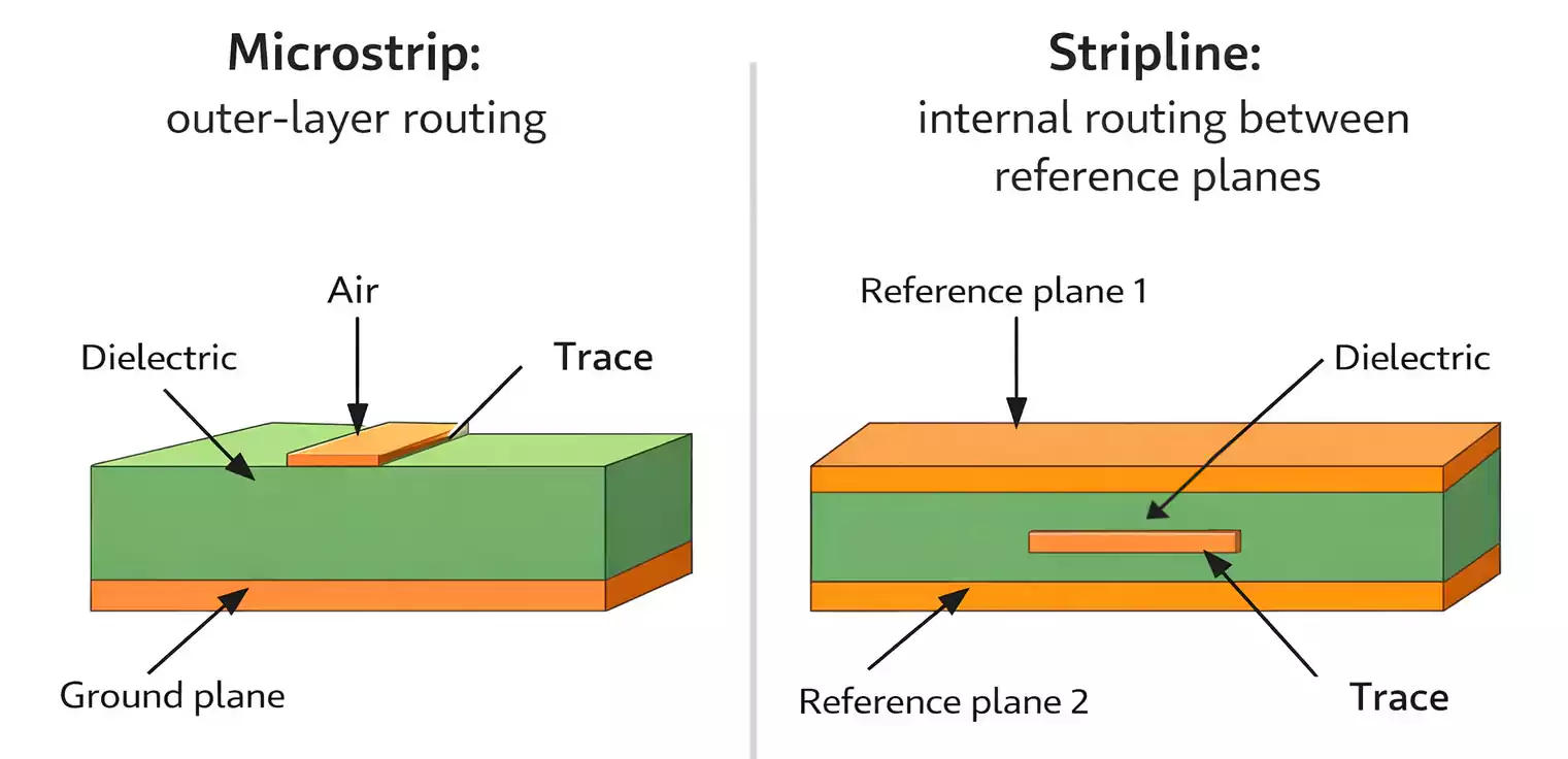
What Is a Microstrip?
A microstrip is a trace routed on the outer layer of the PCB above a reference plane, usually ground.
Because the trace is exposed to air on one side and dielectric material on the other, its electromagnetic field exists partly in air and partly in the substrate.
What Is a Stripline?
A stripline is a trace routed on an inner layer between two reference planes.
Its field is more fully contained within the dielectric, providing a more shielded and controlled environment.
Why This Matters
These are not just ordinary traces. At RF and high-speed frequencies, they behave as transmission lines.
That means their electrical behavior depends on geometry, including:
- trace width
- copper thickness
- dielectric thickness
- dielectric constant (Dk)
- reference plane placement
Microstrip vs Stripline: Key Differences
| Trace location | Outer layer | Inner layer |
| Reference planes | One | Two |
| Field environment | Partly in air, partly in dielectric | Mostly inside dielectric |
| Shielding | Lower | Higher |
| EMI radiation | Higher | Lower |
| Accessibility | Easy to probe and rework | Harder to access |
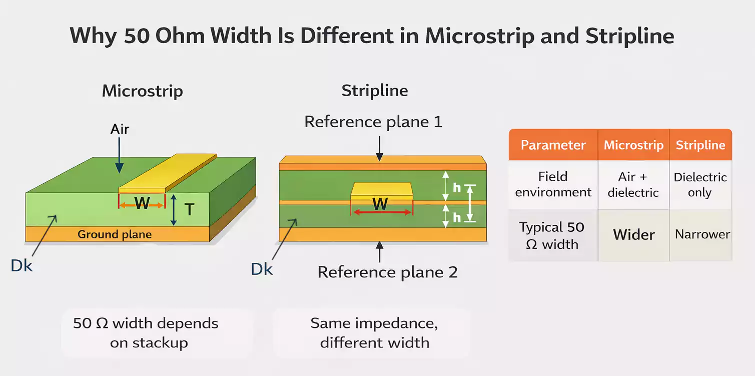
| Typical 50 ohm width | Usually wider | Usually narrower |
| Routing density | Lower | Higher |
| Manufacturing complexity | Lower | Higher |
| Best for | Antenna feeds, launches, tuning | Internal RF routing, isolation, dense multilayer boards |
The Core Difference: Surface Routing vs Internal Routing
The main difference is where the trace is routed.
- Microstrip is routed on the outer layer.
- Stripline is routed on an inner layer between reference planes.
This directly affects shielding, radiation, accessibility, and routing behavior.
Because microstrip is on the surface, it is easier to probe, inspect, and adjust during development, but it is also more exposed to external noise and radiation.
Because stripline is embedded inside the board, it is better shielded and usually radiates less, but it is harder to access after fabrication.
How the Field Behaves in Each Structure
The electrical difference between microstrip and stripline starts with the field distribution.
In a microstrip, part of the electromagnetic field propagates through the PCB dielectric, while the rest propagates through the surrounding air. As a result, the signal sees an effective dielectric constant rather than just the laminate Dk. This is one reason microstrip behaves differently from stripline, even when the trace widths look similar.
In a stripline, the field is more fully confined inside the dielectric between two reference planes. That gives stripline a more contained electromagnetic environment, which generally improves shielding and makes routing behavior more stable in dense boards.
This field difference affects several important design factors, including impedance, propagation speed, loss, radiation, crosstalk, and routing constraints.

Why the Same 50 Ohm Width Does Not Work for Both
A common RF PCB mistake is assuming that 50 ohms corresponds to one fixed trace width. It does not.
A 50 ohm microstrip and a 50 ohm stripline usually require different widths, even on the same board. The reason is simple: they operate in different electromagnetic environments, so the same geometry does not produce the same impedance.
The required width depends on several variables:
- target impedance
- transmission line structure
- dielectric thickness
- dielectric constant (Dk)
- copper thickness
- nearby ground copper
- fabrication tolerance
In many stackups, microstrip ends up wider, while stripline is narrower for the same target impedance. That is why reusing a 50 ohm width from another project is unreliable unless the stackup is essentially the same.
What Actually Determines Controlled Impedance?
Controlled impedance is not created by width alone. It comes from the interaction of the trace geometry, the dielectric environment, and the reference plane arrangement.
Trace width is still one of the most visible variables, but it is only part of the picture. Dielectric height, copper thickness, Dk, and stackup symmetry all influence the final result. Manufacturing tolerance matters too, because even a correct design can drift off target if fabrication variation is not taken into account.
In practice, the main variables are:
- Trace width, which generally lowers impedance as it increases
- Dielectric height, which usually raises impedance when the trace is farther from the reference plane
- Copper thickness, which changes the effective conductor shape
- Dielectric constant (Dk), which usually lowers impedance as it increases
- Stackup symmetry is especially important in stripline structures.
- Manufacturing tolerance, which affects the real built geometry
In other words, impedance control is a stackup problem first and a routing problem second.
Microstrip vs Stripline Loss
This comparison is often oversimplified. There is no universal answer to which structure has lower loss, because the answer depends on which type of loss dominates in the design.
Microstrip can have lower dielectric loss in some cases because part of its field is in air rather than entirely in the substrate. Stripline, however, is better shielded and usually radiates less, which can improve overall signal behavior in dense or noisy layouts.
Total loss depends on more than structure alone. It is shaped by material properties, copper condition, geometry, frequency, and the surrounding board environment. The most important factors usually include:
- frequency
- substrate material
- Dk and Df
- copper roughness
- conductor geometry
- field confinement
So instead of asking which one has the lowest loss, it is more useful to ask which loss mechanism matters most in the design.
EMI, Shielding, and Crosstalk
If EMI control is a priority, stripline usually has the advantage.
Because it is routed between two reference planes, stripline is naturally better shielded from the outside environment. That usually means lower radiation, lower susceptibility to external noise, and better isolation in dense routing areas. This is one of the main reasons stripline is often preferred in multilayer RF and mixed-signal boards.
Microstrip is more exposed, so it is more likely to radiate and interact with nearby structures. That does not make it a poor choice, but it does mean the surrounding layout matters more.
Good EMC still depends on fundamentals such as:
- return path continuity
- solid reference planes
- spacing to nearby conductors
- clean layer transitions
Signal Speed and Delay
Microstrip signals usually propagate faster than stripline signals because the effective dielectric constant seen by a microstrip is lower due to the air interface.
A stripline with more of its field contained within a dielectric usually has slower propagation and a different electrical length for the same physical distance. That difference becomes important in phase-matched RF paths, timing-sensitive interconnects, and length-matched high-speed routing.
So even when two traces have the same physical length, they may exhibit different electrical behavior if one is microstrip and the other is stripline.
Manufacturing, Testing, and Rework
From a practical engineering standpoint, microstrip is usually easier to work with. Because it is routed on the outer layer, it is easier to inspect, probe, tune, and rework during development. That makes it especially useful for prototypes, antenna sections, and RF front-end layouts where access is critical.
Stripline is more demanding because it depends on multilayer fabrication and tighter stackup control. A narrow internal trace geometry can also place greater pressure on manufacturing tolerances. Once the board is built, internal traces are harder to access directly for testing or modification.
In general:
- Microstrip is easier to inspect and debug
- Stripline is better contained but harder to access after fabrication.
When to Choose Microstrip
Microstrip is usually the better choice when the RF path must remain on the surface, or accessibility is important during development.
Typical use cases include antenna feed lines, connector launches, short RF interconnects, and outer-layer matching networks. It also makes sense in circuits that need tuning or probing, or in lower-layer-count RF boards where a simpler structure is preferred.
Choose microstrip when surface routing, easier debugging, and direct access to RF components or antennas are more important than maximum shielding.
When to Choose Stripline
Stripline is usually the better choice when field containment and isolation matter more than accessibility.
It is commonly used in dense multilayer RF PCBs, internal RF routing, mixed-signal boards with noise concerns, telecom systems, radar boards, and other high-frequency designs with tighter EMI requirements. Because the signal is routed between reference planes, stripline usually provides better shielding, lower crosstalk, and cleaner internal routing behavior.
Choose stripline when the design benefits more from shielding and routing density than from easy physical access.
When CPWG Is a Better Option
In many RF layouts, the real decision is not only microstrip vs stripline. A coplanar waveguide with ground (CPWG) is often a third option worth considering.
CPWG is an outer-layer structure like a microstrip, but it adds grounded copper on both sides of the trace. This changes the field distribution and improves confinement, making outer-layer RF routing more controlled. It is often used when the design needs the accessibility of surface routing, but better isolation than standard microstrip can provide.
CPWG is especially useful when you need:
- stronger field confinement
- better isolation on the outer layer
- easier RF access than stripline
- more control than standard microstrip
One important point is that once the side ground is close enough to influence the field, the trace should no longer be treated as a simple microstrip.
A Practical Mixed-Stackup Strategy
Many RF PCBs use multiple transmission line structures. In practice, that is often the most effective approach.
A common strategy is to use microstrip for antenna feeds, launches, and short surface routes; stripline for longer internal routes that require isolation; and CPWG for outer-layer RF routing that needs extra confinement.
This mixed approach is often more realistic than forcing the entire design into a single structure, since different parts of the board often have distinct electrical and mechanical priorities.
Common Design Mistakes
Here are some of the most common mistakes engineers make when comparing or using microstrip and stripline:
1. Using the Same Width for Both
The same impedance target does not mean the same width.
2. Choosing Structure Before Defining the Stackup
Impedance depends on stackup, not just the trace itself.
3. Ignoring Return Path Continuity
A well-sized trace can still perform poorly if the return path is broken.
4. Choosing Stripline Without Checking Manufacturability
Narrow internal traces may increase the risk of fabrication.
5. Choosing Microstrip Without Considering EMI
Surface routing is easier, but it is also more exposed.
6. Treating CPWG as an Ordinary Microstrip
Nearby side ground changes the field behavior and impedance.
FAQ
Is microstrip better than stripline for an RF PCB?
Not always. Microstrip is usually better for surface routing and accessibility, while stripline is better for shielding and lower radiation.
Why is stripline usually narrower for the same impedance?
Because more of its electromagnetic field is confined in the dielectric, which changes the impedance relationship compared with the microstrip.
Does a microstrip always have lower loss?
No. Microstrip may have lower dielectric loss in some cases, but total loss also depends on frequency, material, and structure.
Is stripline always better for EMI?
Usually, yes. Stripline is better shielded, but EMI performance still depends on stackup, return path continuity, and layout quality.
When should I use CPWG instead of microstrip?
Use CPWG when you need outer-layer routing with better field confinement and isolation than standard microstrip.
Can one RF PCB use both microstrip and stripline?
Yes. Many RF PCBs use microstrip for surface routing and stripline for shielded internal routing.
Final Thoughts
Microstrip and stripline serve different purposes in RF PCB design. Microstrip is typically used where surface access, antenna routing, or easier tuning matters. Stripline is usually preferred where shielding, lower radiation, and dense internal routing are more important.
In practice, many RF PCBs use both. The right choice depends on the stackup, signal path, EMI requirements, and manufacturing constraints.
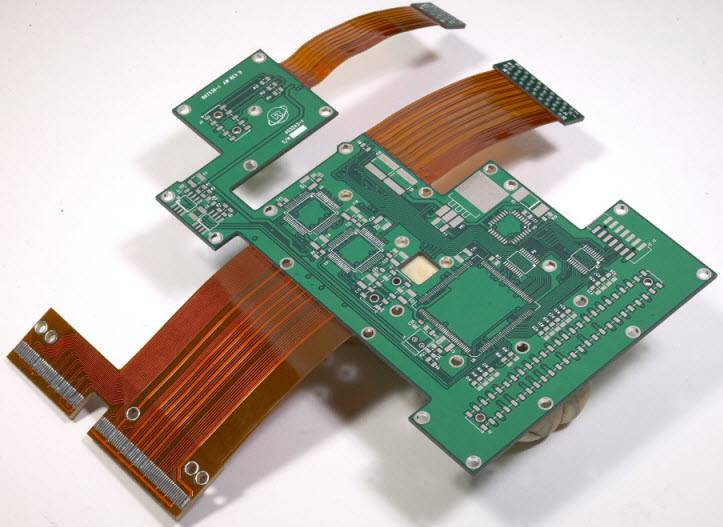
FastTurnPCB supports high-frequency PCB manufacturing, including controlled-impedance multilayer boards built for RF and microwave applications.
