

PCB Accelerometer design is about more than sensor connectivity. In real-world applications, PCB layout directly impacts measurement accuracy, stability, and repeatability.
Unlike ordinary digital ICs, MEMS accelerometers are sensitive not only to motion, but also to PCB flex, thermomechanical stress, nearby heat sources, vibration, and assembly-related effects.
That is why accelerometer PCB design must be approached from both electrical and mechanical perspectives. Sensor placement, footprint design, routing symmetry, and assembly quality all play a critical role in overall performance.
Why PCB Accelerometer Design Is Different
PCB Accelerometer design is not the same as routing a standard digital IC. Because the sensor measures physical motion, it is also sensitive to the physical condition of the PCB itself.
Board flex, localized mounting stress, and nearby heat sources can all affect sensor output. In some cases, the accelerometer may register these effects as offset drift, added noise, or false motion.
That is why PCB layout matters so much. A logic device may tolerate minor layout issues with little visible impact. An accelerometer usually will not.
Common board-related problems include:
- offset instability
- false motion readings
- higher noise
- temperature drift
- Inconsistent results between prototypes and production builds
The main point is simple: in an accelerometer design, the PCB is part of the sensing system.
Choose the Right Accelerometer Before Starting the Layout
A good layout starts with the right sensor. The best choice depends on the application, required performance, and system constraints.
Typical applications include:
- Wearables: low power and compact size
- Robotics: stable output and good dynamic response
- Tilt sensing: low-noise performance at low speed
- Industrial monitoring: higher range and better mechanical robustness
- Consumer devices: small package and simple MCU integration
Before finalizing the layout, review the key specifications:
| Measurement range | Defines how much motion or shock the sensor can detect |
| Noise density | Affects small-signal accuracy |
| Bandwidth / ODR | Should match the target motion profile |
| Interface | I2C is simple; SPI can offer better speed and robustness |
| Package size | Smaller packages save space but may be more layout-sensitive |
If the design only needs linear motion, tilt, or wake-up detection, a standalone accelerometer is usually enough. If it also needs rotation data or sensor fusion, an IMU may be the better fit.
Best Placement for an Accelerometer on a PCB
Placement is usually the most important decision in PCB Accelerometer design. A well-placed sensor can improve stability and accuracy before routing begins.
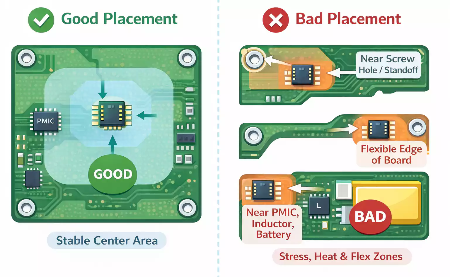
Keep the sensor away from mechanical stress
Avoid placing the accelerometer near:
- screw holes
- standoffs
- snap-fit features
- shields
- enclosure pressure points
These areas often experience localized force during assembly, which can shift the sensor offset.
Avoid flexible board regions
Do not place the sensor near:
- board edges
- narrow extensions
- cutout-adjacent areas
- unsupported corners
- cantilevered sections
These regions are more likely to bend or vibrate during handling and operation.
Stay away from heat sources
Keep the accelerometer away from:
- processors
- PMICs
- charging circuits
- batteries
- high-current traces
- power inductors
Local heating can increase drift and reduce measurement stability.
Watch for vibration sources
Nearby components can inject unwanted mechanical noise into the board, including:
- speakers
- haptic motors
- fans
- relays
- switching power stages
The best placement is usually a mechanically stable, thermally quiet area away from mounting stress and vibration sources.
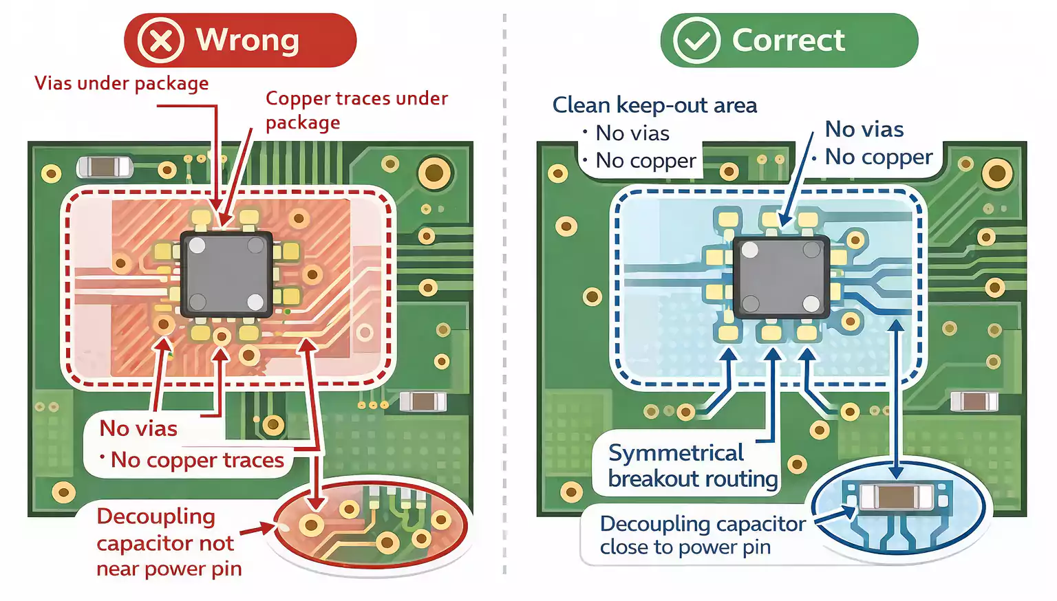
Footprint Design Rules for PCB Accelerometers
Once placement is fixed, footprint design becomes the next priority. For MEMS sensors, the footprint affects both soldering quality and mechanical stress.
Use the recommended land pattern
Always start with the sensor manufacturer’s official package guidance, including:
- land pattern
- pad dimensions
- solder mask definition
- stencil recommendations
- assembly notes
Do not reuse a footprint that looks similar without checking the datasheet.
Do not place vias under the package
Avoid putting these directly under the sensor:
- vias
- top-layer traces
- dense copper features
- mechanical structures
These can affect flatness, create local stiffness differences, and increase thermomechanical stress.
Keep the sensor area clean
A clean layout around the package improves both assembly consistency and long-term stability. It also makes inspection easier and reduces unwanted stress around the sensor.
Routing Tips: Keep the Layout Balanced
Accelerometer routing is usually not difficult in terms of signal speed, but it still requires careful attention.
The main goal is not exotic routing. The goal is clean, short, and balanced routing.
Power routing
Place the decoupling capacitor as close as possible to the sensor power pin.
Best practices:
- Keep the power trace short
- minimize loop area
- connect ground cleanly
- avoid routing through noisy power regions
Ground strategy
The sensor should be connected to a stable electrical reference.
That means:
- Use a clean ground return path
- avoid noisy current loops near the sensor
- keep switching power noise away from the sensing area when possible
Interface routing
For I2C or SPI:
- keep traces short and direct
- avoid unnecessary detours
- avoid routing through high-noise zones
- Keep the sensor section easy to debug
Use symmetrical pad escape routing
Routing symmetry matters more here than many designers expect.
Asymmetrical breakout routing can contribute to uneven stress after reflow. A more balanced escape pattern helps reduce that risk.
2-layer vs. 4-layer boards
Both can work, depending on the product.
2-layer board
- good for simple, compact, cost-sensitive designs
- workable if the electrical environment is relatively quiet
4-layer board
- Often better for mixed-signal stability
- better for designs with wireless modules, processors, or switching power supplies
- easier to maintain a cleaner ground reference
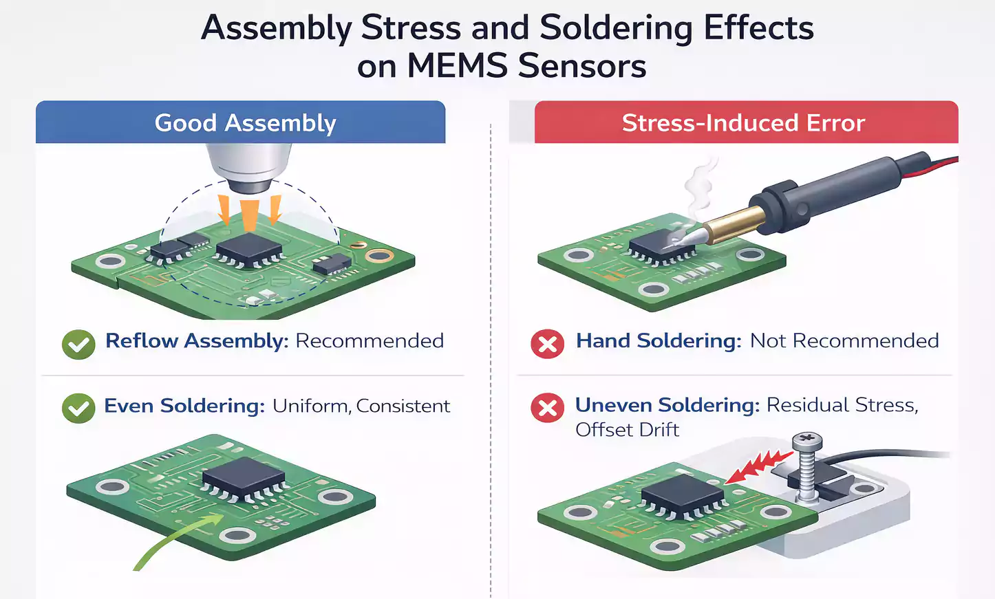
Soldering and Assembly Factors That Affect Accuracy
Assembly can directly affect accelerometer performance. Even with a good layout, poor soldering conditions can reduce accuracy and repeatability.
Reflow is usually preferred
Most MEMS accelerometers are intended for automated reflow assembly. Hand soldering can introduce uneven heating, residual stress, and inconsistent joint formation.
Solder paste consistency matters
Uneven paste deposition can cause the package to seat non-uniformly, leading to offset variation or assembly-induced stress.
Leave room around the sensor
Do not crowd the sensor with heavy parts, fasteners, or large mechanical features. The layout should remain mechanically reasonable in the final product, not just in CAD.
Expect some post-assembly shift
Small offset changes after reflow or final enclosure assembly are common. The goal is to reduce these effects through layout and verify them during testing.
Post-Assembly Checks and Basic Calibration
After assembly, the board should be evaluated as a motion-sensing system—not just as a powered PCB.
First bring-up checks
Start with the basics:
- Confirm that the power is stable
- Verify communication with the sensor
- Read the device ID or status registers
- Confirm axis mapping in hardware and firmware
Static output sanity check
With the board resting still, check whether the accelerometer output makes sense for the board orientation.
This helps catch:
- major offset issues
- axis mapping mistakes
- assembly-related mounting problems
Basic calibration
For many consumer products, a simple firmware offset calibration is enough.
For more demanding designs, a fuller calibration process may be needed to account for:
- system-level alignmente.
- enclosure effects
- board mounting
- temperature behavior
Common PCB Accelerometer Design Mistakes
The most common mistakes include:
- Placing the sensor near screw holes or standoffs
- Putting the sensor next to hot components
- Routing vias or traces under the package
- Ignoring board flex near edges or cutouts
- Using asymmetrical breakout routing
- Hand soldering a reflow package
- Skipping post-assembly validation
These issues are easy to miss because the board may still power up and communicate normally. The real problems often appear later as drift, noise, or unstable readings.
Final Thoughts
A reliable PCB Accelerometer depends on more than electrical connectivity. Layout decisions directly affect how accurately the sensor responds to real motion.
In practice, good performance comes down to a few fundamentals: proper sensor placement, a clean footprint, balanced routing, controlled assembly, and post-build validation.
When these basics are handled well, the board is easier to calibrate, more stable in operation, and more consistent over time.
At FastTurnPCB, we know that precision sensor boards require more than standard PCB layout practices. For accelerometer and other motion-sensing designs, manufacturable layout and mechanical awareness are key to reliable results.