


As electronics continue to shrink while adding more functionality, PCB routing has become increasingly challenging. Higher I/O counts, finer pitch components, and tighter layouts are pushing traditional through-hole board structures to their limits.
This is where HDI PCB technology stands out.
If you are wondering what is HDI PCB, it is a high-density interconnect approach that uses microvias, blind and buried vias, and sequential build-up structures to increase routing density in a smaller footprint. In modern electronic design, HDI PCBs are widely used to improve space utilization, support complex interconnections, and deliver better electrical performance.
What is HDI PCB?
An HDI PCB (High-Density Interconnect printed circuit board) is a multilayer board built with finer traces, tighter spacing, and smaller via structures than a conventional PCB. It typically uses laser-drilled microvias, including blind and buried vias, to increase routing density in a smaller area.
Compared with traditional PCBs, HDI boards offer:
- Finer traces and pads
- Tighter layer-to-layer interconnections
- Smaller via structures
- Better support for high-I/O and fine-pitch components
- More routing capacity in less space
In practical terms, an HDI PCB allows designers to fit more connections into a smaller footprint while improving layout efficiency and electrical performance.
What Is a Microvia PCB?
A microvia PCB is an HDI PCB that uses small laser-drilled vias to create dense layer-to-layer connections. These microvias are usually blind vias, meaning they connect only specific layers rather than passing through the entire board.
Compared with traditional through-hole vias, microvias occupy less space within the PCB and enable more efficient high-density routing. That is why they are widely used in compact, high-I/O, and fine-pitch designs.
Key characteristics of microvias include:
- Small via size
- Usually blind rather than through-hole
- Used for dense interlayer connections
- Better routing efficiency in limited board space
In short, microvias are one of the key structures that enable HDI PCB design.
Why Is HDI PCB Technology Becoming More Important?
HDI PCB technology is becoming increasingly important as modern electronics demand greater performance in less space. As devices get smaller and more complex, traditional PCB structures often struggle to keep up.
Several trends are driving wider HDI adoption:
1. More components in less space
Modern boards often need to fit more components on both sides, leaving less routing space.
2. Smaller packages and finer pitch
As component packages shrink and pitch becomes tighter, routing becomes more difficult, and space efficiency becomes more important.
3. Higher I/O counts
Many devices now combine smaller footprints with higher I/O density, making fan-out and interlayer connections more challenging.
4. Higher performance requirements
High-speed and high-frequency designs require shorter signal paths, better signal integrity, and lower parasitic effects.
Because of these demands, HDI PCB technology is now widely used in smartphones, wearables, automotive electronics, industrial systems, and other compact, high-performance products.
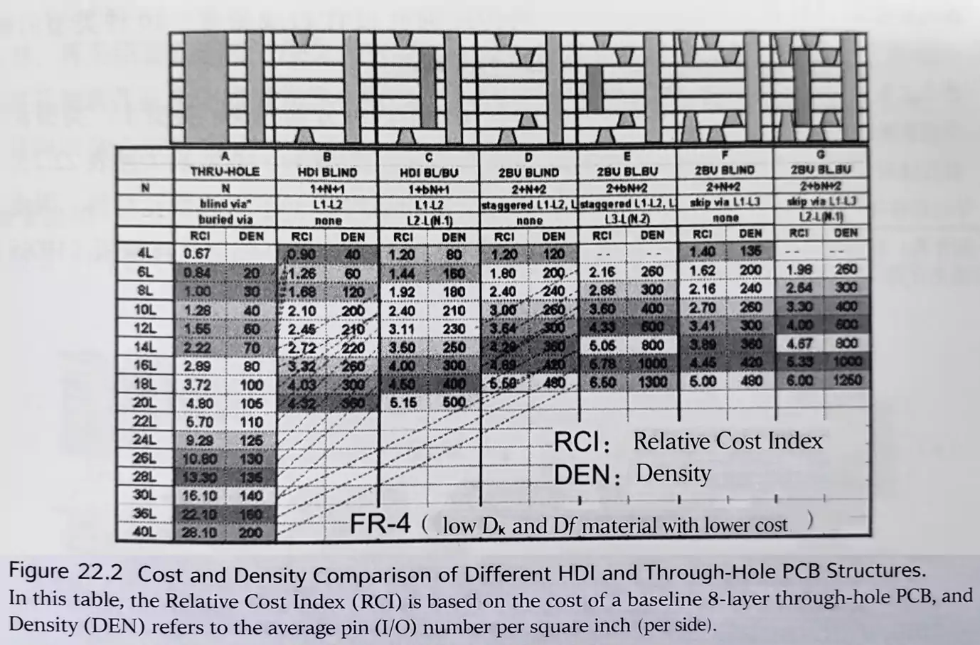
HDI PCB vs Traditional PCB
The most fundamental difference in HDI PCB vs traditional PCB design lies in the interconnection structure and routing efficiency.
1. Traditional PCB structure
Traditional multilayer boards mainly rely on mechanically drilled through-holes for layer-to-layer interconnection. This is a mature and cost-effective method, but it becomes limiting in high-density designs because:
- Through-holes consume valuable routing channels.
- Escaping high-I/O packages becomes more difficult.
- More board layers may be required.
- Small form factors are harder to achieve without tradeoffs.
2. HDI PCB structure
An HDI PCB uses microvias, blind and buried vias, and sequential build-up structures to improve routing flexibility. Key advantages include:
- Smaller via footprints
- Easier fan-out for dense components
- Less routing blockage inside the board
- More interconnections in a smaller area
- The potential to reduce layer count or shrink board size
So an HDI PCB is not just a replacement for traditional PCB design. It is a more effective solution for designs where density, size, and performance all matter at once.
HDI PCB Benefits
The value of an HDI PCB goes beyond higher routing density. It also helps improve product size, layout efficiency, and electrical performance.
1. Higher routing density
Microvias and fine-line structures allow more connections in a smaller area, which is the main advantage of HDI.
2. Smaller and lighter products
By using board space more efficiently, HDI can help reduce PCB size and support more compact end products.
3. Better support for high-I/O packages
HDI is well-suited for BGAs and other high-pin-count components that require efficient fan-out and escape routing.
4. Improved electrical performance
Shorter interconnect paths and more compact routing can help reduce parasitics, lower delay, and improve high-speed signal behavior.
5. Better EMI and RFI control
A tighter and more optimized interconnect structure can also help reduce electromagnetic and radio-frequency interference.
6. Higher system integration
HDI makes it easier to fit more functions into a smaller board area, which is critical for compact, high-performance electronics.
Is HDI PCB Manufacturing Always More Expensive?
Not always.
From a fabrication standpoint, HDI PCB manufacturing is more complex than standard through-hole construction. But at the system level, HDI can often deliver better overall value.
An HDI design may allow:
- Fewer board layers
- Smaller board size
- Higher routing capacity
- Better electrical performance
- Greater component integration
In high-density designs, a traditional through-hole PCB may require more layers and more board area, yet still impose routing limitations. In those cases, HDI can be the more practical and cost-effective solution.
The real cost comparison should consider more than just the fabrication price. Board size, layer count, performance, and design feasibility all matter.
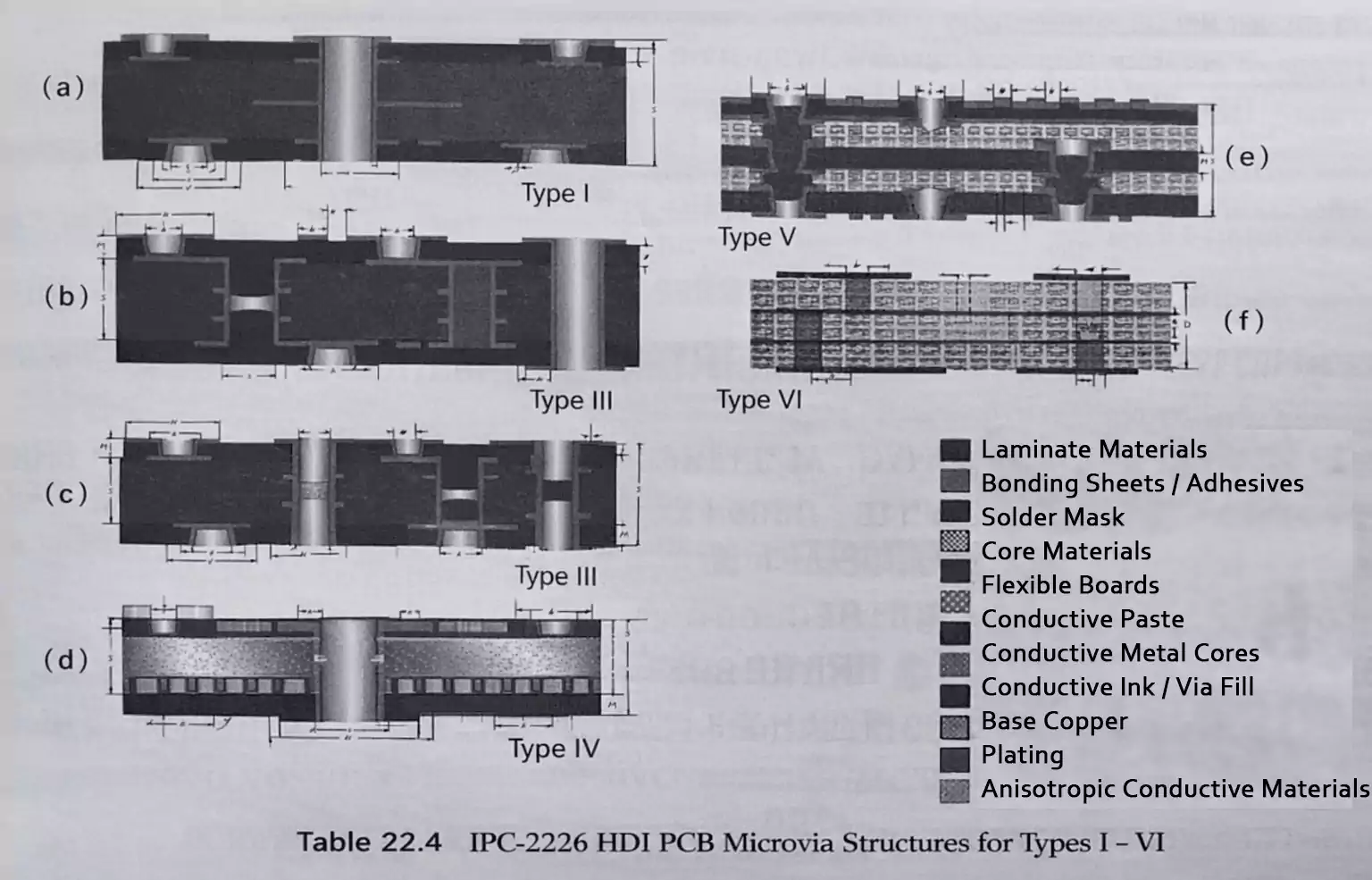
Common HDI PCB Structures
Most HDI structures can be understood through a few core building blocks.
1. Microvia
A small via used for high-density interconnections. This is the foundation of most HDI designs.
2. Blind via
A via that connects an outer layer to one or more inner layers without passing through the full board thickness.
3. Buried via
A via located only between inner layers, with no visible opening on the outer surfaces.
4. Sequential build-up
A manufacturing method that adds dielectric and conductor layers step by step, forming microvia connections as the structure builds.
In practical terms, these structures help free up routing space and enable dense interconnections.
HDI PCB Manufacturing: What Matters Most?
The most important technology in modern HDI PCB manufacturing is laser drilling.
Compared with mechanical drilling, laser drilling is better suited for:
- Smaller via sizes
- Higher interconnect density
- Finer layer-to-layer structures
That is why laser-drilled microvias are now a core feature of most HDI boards.
Still, HDI manufacturing involves more than via formation. A successful HDI process also depends on material selection, stack-up design, metallization, lamination, and reliability control.
What Applications Are HDI PCBs Best Suited For?
HDI PCBs are widely used in products that require high density, small size, and strong electrical performance, including:
- Smartphones
- Tablets
- Wearables
- Automotive electronics
- Medical devices
- Communication equipment
- Industrial systems
- High-speed and high-frequency products
In general, when a design requires compact size, high I/O density, and efficient routing, HDI is a strong fit.
HDI PCB Design: What Should Designers Focus On?
HDI PCB design is not just about fitting the routing. It also needs to balance manufacturability, reliability, and cost.
Key design considerations include:
- Microvia structure and stack-up matching
- Routing density planning
- Material properties
- Lamination strategy
- Reliability requirements
- Cost-performance tradeoffs
A good HDI design is not about pushing every feature to the minimum. It is about choosing the right structure for the product, the manufacturing process, and the target cost.
What IPC Standards Are Commonly Used for HDI PCB Design and Manufacturing?
When an HDI design moves into production, IPC standards are commonly used as references. Key documents include:
- IPC-2226: Design standard for HDI structures
- IPC-4104: Material specifications for HDI structures
- IPC-6016: Qualification and performance specification for HDI structures
- IPC-2315: Design guide for HDI structures
HDI PCB technology is supported by a well-established framework of design, material, and performance standards.
Final Thoughts
An HDI PCB enables higher routing density, smaller board size, and better electrical performance within a single design approach.
Compared with a traditional PCB, the advantage of HDI is not just smaller vias. It is a more efficient interconnection strategy for today’s compact, high-I/O, high-performance electronic products.
When conventional through-hole routing starts to limit the design, HDI is often the solution that enables the layout.
