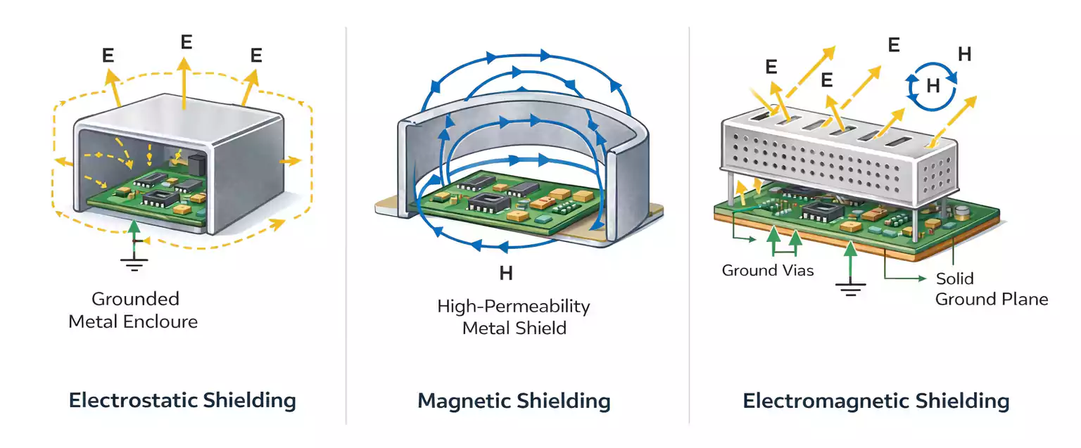
As electronic devices become smaller, faster, and more integrated, EMI has become a more important design concern. High-speed signals, RF circuits, switching power supplies, and wireless modules can all create interference that affects nearby components and overall system performance.
For that reason, EMI shielding is now a standard part of electronic product design. It helps improve signal quality, reduce interference, and support EMC compliance.
Among the most common EMI shielding methods, EMI shield cans and conductive coatings are two widely used solutions. Shield cans are typically used for localized PCB protection, while conductive coatings are often applied to the inner surfaces of plastic enclosures for broader shielding coverage. This article explains how both methods work, where they fit best, and what design factors matter most.
Why Electronic Products Need EMI Shielding
Modern electronic devices contain many sources of electromagnetic interference, including RF circuits, power amplifiers, clock signals, high-speed interfaces, and switching power supplies. At the same time, antennas, display modules, analog front ends, and other low-level signal paths are often sensitive to external noise.
Without proper isolation, interference can reduce wireless performance, introduce noise, cause display issues, create data errors, and affect system stability. It can also increase the difficulty of EMC troubleshooting and compliance testing.
For this reason, EMI shielding should be considered early in the design process. An effective solution depends on frequency, mechanical constraints, material selection, and manufacturing requirements.
A Common Solution for Localized Shielding: EMI Shield Cans
What Is an EMI Shield Can?
An EMI shield is a metal structure used to protect a specific area on a PCB, commonly found in smartphones and GPS devices. Its purpose is to reduce radiation from a local circuit block and limit external electromagnetic energy effects on critical components. It is often placed over RF sections, power amplifier circuits, and sensitive areas near an LCD module (LCM).
Structurally, this type of shield usually consists of legs and a cover, assembled together. The cover is often dome-shaped or crown-like, which helps enclose components while fitting within limited internal space.
Common Materials and Assembly Considerations
These parts are typically made from conductive metals. Common options include:
- 0.2 mm stainless steel
- Nickel silver
Nickel silver is often preferred because it is relatively easy to solder, which can simplify assembly.
When an EMI shield can is installed on the PCB through SMT, the design should also consider pick-and-place requirements, including suction or pickup features. This may seem like a small manufacturing detail, but it can affect placement efficiency and assembly yield in production.
Fixed vs. Removable Designs
EMI shield cans are generally available in two configurations: fixed and removable.
Fixed type
A fixed shield can be soldered directly to the PCB through SMT. This provides a stable structure and a direct grounding path, making it well-suited for mass production and areas that do not require later access.
Removable type
A removable version is typically used with the product structure or the LCM or attached to a shielding frame through tabs or formed protrusions. This design is more convenient for debugging, rework, and maintenance.
From an engineering perspective, fixed designs prioritize reliability and production consistency, while removable designs offer better serviceability.
PCB EMI Shielding Can Design: What Matters Most
A PCB EMI shielding may look simple, but its size, thickness, material, and mounting method should all be based on the application.
1. Size and Component Height
The shield must provide enough internal clearance for the components underneath it, especially the tallest ones. If the height is too low, it can create mechanical interference. If it is too large, it wastes internal space and works against miniaturization.
2. Interference Source Strength
Power level directly affects shielding requirements. In a power amplifier section, for example, a higher transmit power level generally increases the chance of interference affecting nearby circuits. That raises the demands on structural integrity, grounding quality, and material performance.
In other words, the question is not only whether shielding is present, but whether it is sufficient.
3. Operating Frequency Range
Shielding performance is closely related to frequency, so the operating band must be clearly defined from the start. Wi-Fi systems, for example, commonly operate at 2.4 GHz and 5.8 GHz. At different frequencies, factors such as metal thickness, opening size, edge gaps, and grounding approach can all affect the final result.
4. PCB Contact and Gap Design
It is often assumed that a metal shield must be tightly attached to the PCB at every point to work effectively. In practice, that is not the only valid approach. If grounding and structural design are handled properly, some gaps can still be acceptable.
For example, beryllium copper spring contacts are widely used in some equipment to provide conductive contact and EMI sealing. This approach offers a useful balance of elasticity, conductivity, and assembly tolerance. In gap design, the goal is not simply to make everything as tight as possible, but to balance mechanical feasibility with electrical performance.
5. Material and Thickness Selection
Select metal type and thickness based on the intended frequency range, as different applications demand varying conductivity, solderability, strength, and cost. In high-frequency designs, consider thickness, grounding path, and opening control together.
Where EMI Shield Cans Work Best
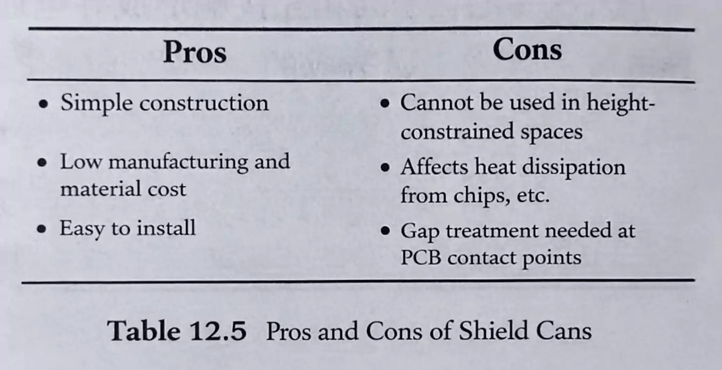
The main advantage of an EMI shield is that it provides targeted protection for a specific circuit area. If one region on the PCB is a major source of interference, or if nearby components are especially sensitive, this approach is often one of the most direct and effective solutions.
That said, it also has limitations. It is generally better suited to products with enough internal space, since the part adds both height and installation requirements. In ultra-thin or highly compact designs, space constraints can make this approach more difficult to implement.
Metal parts also add structural complexity, assembly requirements, and cost. For that reason, they are usually best used as a focused local solution rather than the only shielding method in a product.
A Good Option for Plastic Housings: Conductive Coatings and Conductive Paint
What Is a Conductive Coating?
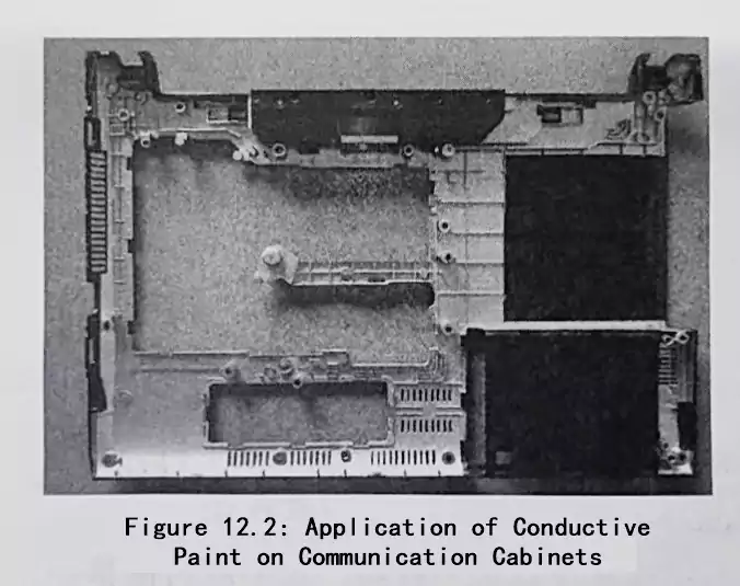
If an EMI shield can is mainly used for local PCB protection, a conductive coating is better suited for shielding the enclosure itself. A conductive coating is a sprayable functional layer that forms an electrically conductive film after drying, allowing it to block electromagnetic energy.
Conductive coatings are made by dispersing metal powder into a resin system. Once sprayed and cured on the inner surface of a plastic enclosure, the coating provides metal-like shielding.
In many applications, this type of material is also referred to as conductive paint or an EMI shielding coating.
Why This Method Has Become More Common
Compared with metal structural parts, a spray-applied coating is easier to use on complex surfaces and irregular housing shapes. It also works well in products built around plastic enclosures. Its main advantages include:
- Good electrical conductivity
- High EMI shielding effectiveness
- A simple application process similar to standard spraying
- Only a thin layer is needed on the inside of the housing.
- Less pressure on space, assembly, and cost
- A practical way to create a metallized effect on plastic parts
Because of these advantages, conductive paint and other coating-based solutions have increasingly replaced older methods such as tin foil, copper foil, and some traditional metal shielding structures in certain applications.
Common Application Areas
This type of EMI shielding coating is widely used in many electronic products, including:
- Communication products such as mobile phones
- Laptop computers
- Portable electronic devices
- Consumer electronics
- Network hardware, such as servers
- Medical instruments
- Household electronics
- Aerospace and defense systems
In all of these products, the plastic enclosure itself does not provide conductivity or shielding. The coating helps close that gap.
What Is Often Overlooked When Using Conductive Paint or Coatings
Although the process may look similar to ordinary spray painting, stable conductivity depends heavily on process control.
1. Thorough Mixing Before Use
A conductive coating should be mixed thoroughly before application so the metal particles are evenly dispersed. If they are not, the dried film can develop weak areas and inconsistent shielding performance. In nickel-based systems, for example, poor particle dispersion can lead to an unstable conductive network.
2. Stirring After Thinning
Once the material has been thinned, the metal content can settle more easily, so frequent stirring during use is important. In practice, the interval is typically limited to 5 minutes or less. This helps maintain a uniform composition during spraying and reduces performance variation across the coated surface.
Thinned material should also be used as soon as possible rather than stored for long periods. Even if some sedimentation occurs, the coating can usually still be used after remixing, provided the material has not otherwise degraded.
3. Safety and Environmental Control
During application, the work area should be well ventilated, and long-term direct contact or inhalation should be avoided. Leftover material and waste liquid should not be discharged into drains or waterways.
These may sound like basic shop rules, but they are just as important in prototyping as they are in full production.
How to Choose Between a PCB EMI Shielding Can and an EMI Shielding Coating
From an engineering standpoint, these two methods do not replace each other. They address different shielding needs at different levels of the product.
If the goal is to isolate RF sections, power amplifiers, high-speed signals, or other sensitive PCB areas with localized protection, a PCB EMI shielding can usually be the better choice. It is especially effective for controlling radiation and coupling around a specific circuit block.
If the product uses a plastic enclosure and needs broader housing-level shielding without adding too many metal structural parts, an EMI shielding coating is often the more flexible option. It integrates more easily with enclosure geometry and industrial design.
A simple way to think about it is:
- For localized PCB shielding, start with an EMI shield can
- For the inner surface of a plastic enclosure, start with a conductive coating.
If the product has both strong local interference sources and system-level shielding requirements, both methods can be used together.
Conclusion
There is no one-size-fits-all solution to EMI control. The right approach depends on the product structure, operating frequency, and source of interference.
For localized PCB shielding, an EMI shield can remain a practical and proven option, especially around RF sections, key circuits, and display-related areas. For plastic housings, a conductive coating or conductive paint provides a more flexible way to add shielding without introducing extra metal structures.
In many designs, the best result comes from choosing the right method for the right part of the product. Good EMI performance depends not only on material selection, but also on sound design decisions and consistent process control.