In electromagnetic compatibility (EMC) design, PCB EMI shielding is one of the most basic yet most important techniques. It helps reduce external interference and also prevents internal circuits from radiating unwanted noise. In PCB design, high-frequency circuits, analog systems, RF modules, and power electronics, shielding often directly impacts stability, reliability, and EMC test performance.
Many engineers think of electromagnetic shielding as simply adding a metal cover. In practice, effective PCB shielding involves much more than that. Material selection, grounding, structural continuity, openings, and shielding performance all influence the final result. This article explains the main types of shielding structures, how they work, and how EMI shielding effectiveness is evaluated.
What Is a Shielding Structure?
A shielding structure is a conductive or magnetic material used to block, reduce, or control the propagation of electric fields, magnetic fields, or electromagnetic fields. Its purpose is to create a barrier between a noise source and the protected area, so that the interfering field is reflected, absorbed, redirected, or conducted to ground.
Depending on the type of field being controlled, shielding structures are generally divided into three categories:
- Electrostatic shielding
- Magnetic shielding
- Electromagnetic shielding
Each type is designed for a different purpose and relies on different material properties, so they are not interchangeable.
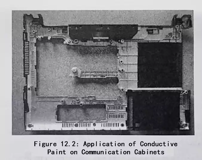
In PCB products, shielding structures are not limited to the outer enclosure. It can also take the form of a local metal shield, a grounded shielding layer, a conductive coating, conductive foam, conductive gasket material, or even the shield around a cable.
The Three Main Types of PCB EMI shielding
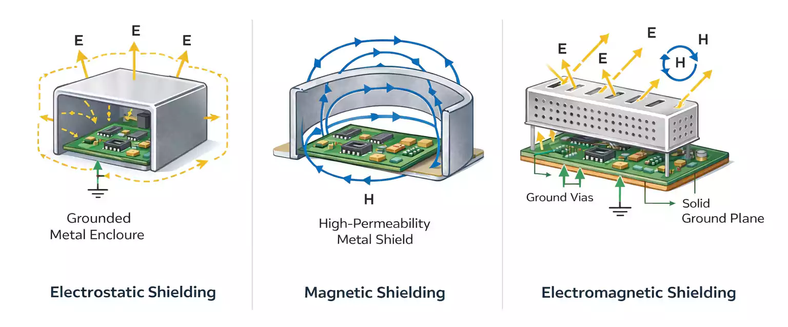
1. Electrostatic Shielding
Electrostatic shielding is used to suppress electric fields.
It is typically made from highly conductive, non-magnetic materials such as copper or aluminum, and it usually requires grounding. Its function is to terminate the electric field at the metal surface and carry accumulated charge to ground, preventing the field from reaching the protected area.
In simple terms, electrostatic shielding depends on three things:
- A good conductive material
- A reliable ground connection
- A structure that keeps the electric field outside the shielded region
When electric-field coupling is the main problem, proper grounding is often just as important as the metal shield itself.
In PCB design, this applies to grounded metal covers, grounded copper areas, and shielded enclosures connected to ground. Without a solid ground path, electrostatic shielding performance drops significantly.
2. Magnetic Shielding
Magnetic shielding is used to control magnetic fields.
It is usually made from materials with high magnetic permeability, such as steel or other ferromagnetic materials. Instead of simply blocking magnetic flux, the shield provides an easier path for magnetic field lines, guiding them through the shielding material instead of allowing them to spread into nearby space.
That means magnetic shielding depends more on permeability than conductivity. This becomes especially important at low frequencies, where ordinary metal covers may do little to address magnetic interference.
In practice, magnetic shielding is often required near transformers, inductors, high-current loops, and circuits sensitive to low-frequency magnetic fields.
3. Electromagnetic Shielding
Electromagnetic shielding primarily reduces the effects of high-frequency electromagnetic fields, making it the most common form of PCB EMI shielding.
High-speed digital circuits, switching power supplies, RF modules, clock circuits, and high-speed interfaces often require this type of protection. Compared with electrostatic and magnetic shielding, electromagnetic shielding works through a more complex combination of mechanisms, including:
- Reflection of electromagnetic waves at the shield surface
- Eddy currents are induced within the shielding material.
- Conduction of interference current to ground
- Absorption and dissipation of high-frequency energy in certain materials
Together, these effects reduce the field strength that reaches the protected area.
In other words, electromagnetic shielding does not rely on a single mechanism. It is usually the result of reflection, loss, absorption, and grounding working together. That is why it is especially important in high-frequency EMI control.
From a PCB engineering perspective, PCB shielding usually appears in three forms:
- Component-level shielding: shielding a single device or noisy component with a metal can
- Board-level shielding: shielding a functional area or a larger section of the PCB
- Cable-level shielding: applying shielding around high-speed or high-frequency cables
EMI Shielding Materials and Material Selection
Choosing the right EMI shielding materials is not just about whether a material is metal. Material selection should match the type of interference, the operating frequency, the mechanical structure, and the cost target.
Common shielding materials include:
- Copper
- Aluminum
- Nickel
- Steel
- Metal foil
- Conductive coatings
- Conductive gaskets
- Conductive tapes
- Ferrite materials
In general, highly conductive materials are better for reflective shielding, high-permeability materials are better for magnetic shielding, and ferrite-based materials are useful for absorbing and suppressing high-frequency noise.
In real products, material selection usually depends on several questions:
- Is the interference mainly electric, magnetic, or electromagnetic?
- What frequency range matters most?
- Does the shield need to be grounded?
- Will the structure need openings for airflow or access?
- Does it also need to provide mechanical strength?
- Are there assembly or cost constraints?
Material choice only makes sense in the context of the full application.
Why Multilayer PCB EMI Shielding Works Better
When a single shield layer is insufficient, multilayer shielding can deliver better performance.
A common approach is:
- Use a high-conductivity outer layer to improve reflection.
- Use a high-permeability inner layer to reduce magnetic losses or improve field containment.
This combination allows different materials to handle different parts of the shielding function.
So, multilayer shielding is not just adding more metal. It is a more deliberate design approach in which each layer serves a different purpose, resulting in stronger overall shielding.
In PCB products, multilayer shielding can also be understood more broadly as a combined strategy, such as:
- A metal shield can work together with a solid ground plane.
- Absorptive materials combined with a conductive enclosure
- Conductive sealing materials are used along grounded edges.
In many cases, shielding performance comes from the entire system rather than a single part.
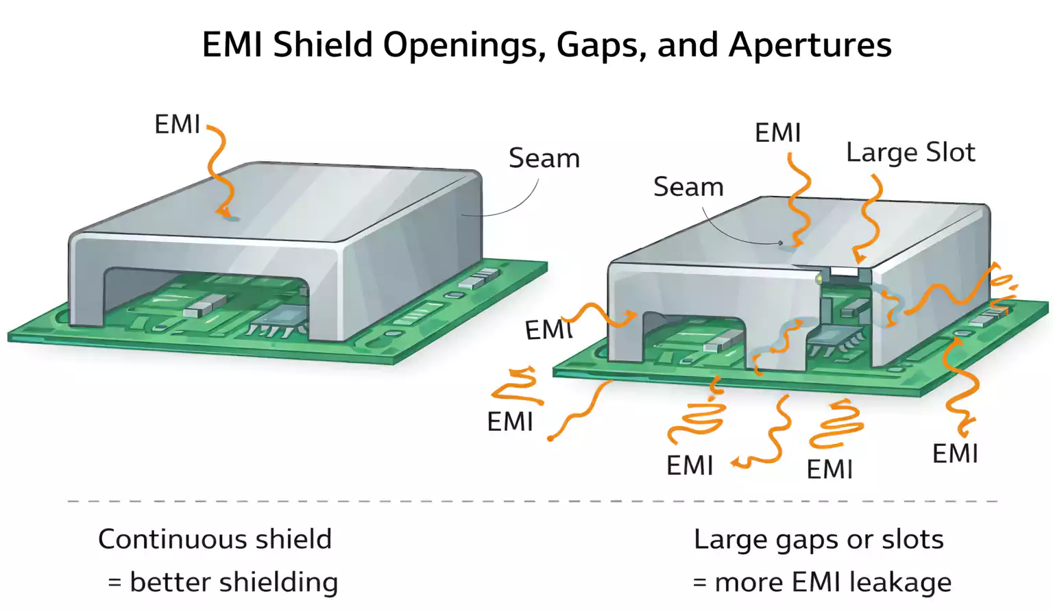
EMI Shield Openings, Gaps, and Apertures
One of the most overlooked problems in PCB EMI shielding design is structural discontinuity.
If the shielding structure contains holes, seams, slots, or EMI shield openings / gaps / apertures, shielding performance can drop significantly. The higher the frequency, the more serious this effect becomes.
The reason is that these discontinuities compromise the integrity of the shielding boundary, creating leakage paths for electromagnetic energy. At high frequencies, a gap or slot can even behave like an unintended radiating structure, worsening EMI coupling or leakage.
This means shielding performance depends not only on the material itself, but also on structural details such as:
- Whether the enclosure is continuous
- Whether seams are tight and well-bonded
- Whether openings are appropriately sized
- Whether the assembly maintains electrical continuity
- Whether cable entry points are properly treated
- Whether the shield has a low-impedance connection to ground
In high-frequency design, these issues are often more important than simply increasing shield thickness.
How to Improve PCB Shielding Performance
Once you understand the impact of gaps and openings, the next step is improving the design.
Common approaches include:
- Making the shield as continuous and enclosed as possible
- Increasing the number of connections between the shield and the ground plane
- Adding ground vias or grounded solder points along the shield boundary
- Using conductive gaskets, conductive foam, or conductive compounds to treat seams
- Filtering or properly terminating cables entering the shielded area
- Avoiding large openings near high-frequency sensitive regions
From an engineering standpoint, effective PCB EMI shielding is not just about placing a metal cover over a circuit. It is about maintaining a continuous, closed, low-impedance shielding path.
What Is EMI Shielding Effectiveness?
To know whether a shielding design is working, you need a way to measure it. Two common ways to describe shielding performance are:
- Shielding coefficient
- Shielding attenuation
Both describe the same basic idea: how much the interfering field is reduced after passing through the shield.
In engineering practice, this is often summarized as PCB EMI shielding effectiveness. It is not determined by only one factor. Material properties, frequency, grounding, structural continuity, openings, and return path design all affect the result.
What Is the Shielding Coefficient?
The shielding coefficient is the ratio between the field strength in the protected area with the shield present and the field strength at the same location without the shield.
In simple terms:
- The smaller the field inside the protected region
- The smaller the ratio compared with the unshielded case
- The better the shielding performance
So, the smaller the shielding coefficient, the better the shielding.
This metric shows how much interference still passes through the shielding structure into the protected area.
What Is Shielding Attenuation?
Shielding attenuation is the reduction in the interfering field caused by the shield, typically expressed in decibels (dB).
It shows how much the field strength has been reduced, making it easier to understand in engineering discussions and test reports.
The rule is simple:
- The larger the shielding attenuation, the better the shielding
A higher dB value means the interference has been reduced more, so the shield is performing better.
In product specifications, EMC reports, and engineering discussions, dB is often the most practical unit for describing PCB EMI shielding effectiveness.
How to Interpret Better Shielding Performance
A good shielding structure can be evaluated in two ways.
From the Shielding Coefficient
- A smaller ratio means fewer fields reach the protected area.
- Therefore, the shielding is better.
From Shielding Attenuation
- A larger attenuation value means the interference is reduced more.
- Therefore, the shielding is better.
Although these two expressions are different, they point to the same conclusion:
The less interference that reaches the protected space, the better the shield performs.
There is one important point to add for PCB design: high EMI shielding effectiveness does not mean a shield alone can solve every EMI problem. If the layout already has serious issues, such as broken return paths, split ground planes, poor decoupling, or sensitive circuits placed too close to noisy ones, adding a shield may only provide limited improvement.
That is why shielding should usually be considered together with:
- Continuous ground planes
- Good layout partitioning
- Short current loops
- Clean return paths
- Proper decoupling
- Ground-via stitching
- Separation between noisy and sensitive regions
In other words, PCB EMI shielding is an important EMC tool, but it is only one part of a complete design strategy.
Key Takeaways
Here are the main points to remember:
- Shielding structures are used to reduce or control electric, magnetic, and electromagnetic fields.
- The three main categories are electrostatic, magnetic, and electromagnetic shielding.
- Electrostatic shielding depends on conductive materials and proper grounding.
- Magnetic shielding depends primarily on high-permeability materials.
- Electromagnetic shielding typically works through reflection, eddy currents, absorption, and grounding.
- In PCB products, shielding often appears at the component, board, and cable levels.
- EMI shielding materials should be selected based on frequency, structure, grounding, and cost.
- Multilayer or combined shielding strategies are usually more effective than a single-layer approach.
- EMI shield openings, gaps, and apertures can reduce shielding performance, especially at high frequencies.
- Shielding performance can be described using the shielding coefficient or shielding attenuation.
- A smaller shielding coefficient means better shielding, while a larger attenuation value means stronger shielding.
- The most effective PCB shielding designs work together with grounding, layout, and structural continuity.
Final Thoughts
Electromagnetic shielding may appear to be a mechanical feature, but it is actually a combination of materials, circuit behavior, grounding, frequency response, and structural design. To build an effective shielding solution, you need to consider the type of field involved, the shielding method, the structure's continuity, and how performance will be evaluated.
For PCB applications, the bigger lesson is that PCB EMI shielding works best as part of a complete EMC strategy. A metal cover by itself is rarely enough. Real performance comes from the shield, the ground plane, the layout, the seams, and the cable treatment, all working together as one coordinated system.