

Designing a PCB in EAGLE CAD involves more than drawing connections. A reliable board starts with a clear schematic, continues with a well-planned layout, and ends with manufacturing-ready files.
This guide covers the complete EAGLE CAD PCB design workflow, from schematic capture to PCB layout and final fabrication output. It is intended for beginners, makers, students, and small hardware teams who want to build better boards with a practical, structured approach.
What Is EAGLE CAD PCB Design?
EAGLE CAD is an electronic design tool used for two main tasks: schematic capture and PCB layout.
The schematic is the logical version of the circuit. It shows how components connect electrically. The PCB layout is the physical version. It defines where parts sit on the board, how traces are routed, how power and ground are handled, and whether the design will be easy to manufacture and assemble.
When someone searches for Eagle CAD PCB design, they are usually looking for a workflow like this:
- Create the schematic
- Choose the right footprints.
- Convert the design into a board.
- Place components in logical positions
- Route traces and apply design rules
- Export Gerber files for fabrication
That is the real core of PCB design in EAGLE.
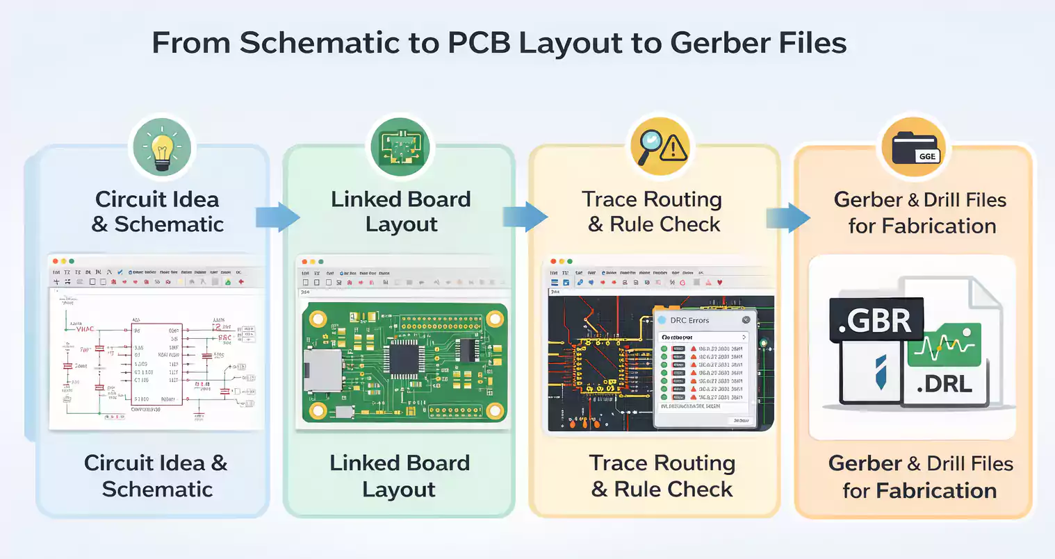
How EAGLE Fits Into the PCB Design Workflow
Most PCB projects start with a circuit idea. Maybe you already know the major building blocks—a microcontroller, voltage regulator, connectors, sensors, LEDs, driver circuits, or communication interfaces.
From there, the process typically moves through three stages.
1. Schematic capture
This is where you define the electrical connections. Which pins connect together? Which parts share power? Where do the pull-up resistors, bypass capacitors, and headers go?
2. PCB layout
This is where the project becomes physical. You decide the board size, component placement, routing paths, copper clearances, and grounding approach.
3. Manufacturing output
Once the board is checked and finalized, you export the files needed for fabrication—usually Gerbers and drill files, and in some cases a BOM and pick-and-place data for assembly.
Many beginner tutorials focus heavily on software actions. That is useful at first, but it only gets you so far. Good PCB design comes from understanding both the tool and the design logic behind it.
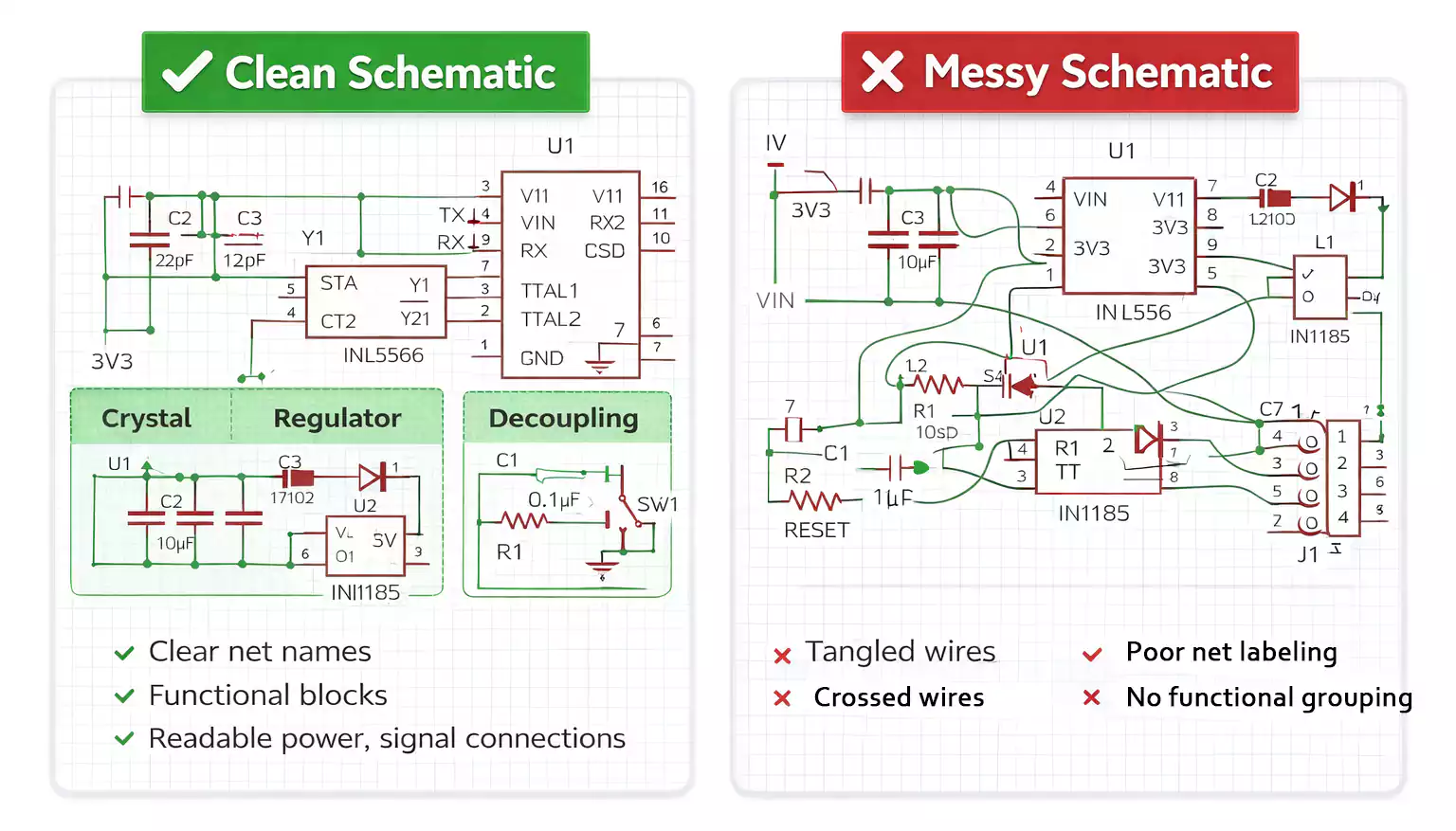
Step 1: Build a Clean Schematic
Every good PCB starts with a good schematic. If the schematic is unclear, incomplete, or built on the wrong parts, the layout stage becomes harder than it needs to be.
Choose the right symbols and footprints
One of the easiest ways to create problems later is to choose a part symbol without checking the footprint. In EAGLE, the logical symbol and the physical package both matter.
For example, selecting a capacitor symbol is not enough. You also need the correct package—such as 0603, 0805, or a through-hole footprint that matches the real part you plan to use. The same goes for ICs, connectors, diodes, crystals, and headers.
Before moving on, make sure:
- The pin count is correct.
- The package matches the real component.
- Pad spacing is accurate.
- polarity and orientation are clear
- The footprint matches the datasheet.
Name nets and organize the circuit clearly
A clean schematic makes the layout much easier. Use meaningful net names for important connections, such as:
- 3V3
- 5V
- GND
- RESET
- SDA
- SCL
- TX
- RX
It also helps to group the circuit into functional blocks. Keep the power, controller, and I/O sections together. This makes the schematic easier to read and gives you a head start when it is time to place components on the board.
Run ERC before layout
Before switching to the PCB view, run ERC (Electrical Rule Check).
ERC helps catch issues such as missing connections, incompatible pin types, and accidental open nets. It is much easier to fix those problems in the schematic than after you have already started laying out the board.
Step 2: Convert the Schematic Into a PCB Layout
Once the schematic is finished and checked, EAGLE can generate the linked board layout view. At that point, the components appear as physical packages, and the electrical connections show up as airwires.
This is where many beginners jump straight into routing. That usually leads to a messy board.
PCB layout is not just “connect the dots.” It is a planning step. You need to think about board size, part placement, routing priority, and real manufacturing constraints.
Start by defining the board outline. Think beyond the circuit itself.
A board that works electrically but does not fit the product still fails the job.
Step 3: Place Components for a Better PCB Layout
Placement has a huge impact on board quality. In many cases, smart placement solves most routing problems before routing even begins.
Start with connectors, ICs, and mechanical constraints
Begin with the parts that have the least flexibility, such as:
- USB connectors
- terminal blocks
- pin headers
- switches
- status LEDs
- mounting holes
- large ICs or modules
These parts are usually tied to enclosure openings, cable access, or user interaction, so their positions should be decided first.
Once those are in place, move on to the main active devices—microcontrollers, regulators, memory chips, driver ICs, and similar components.
Group parts by function
After the fixed-position components are placed, organize the rest of the board by function.
For example:
- Place decoupling capacitors beside the IC they support
- Keep crystals and their load capacitors close to the clock pins.
- Place the regulator feedback parts close to the regulator.
- Keep analog circuitry away from noisy power sections.
- keep connectors reasonably close to the circuits they serve
This approach makes routing cleaner, shortens trace lengths, and usually improves performance.
Keep decoupling capacitors close
This is one of the most important PCB layout habits to learn early.
Decoupling capacitors should be placed as close as possible to the power pins of the IC they support. Their job is to supply local current quickly and reduce noise on the power rail. If they are placed too far away, they become less effective.
On a real board, poor decoupling placement can lead to unstable behavior, noise issues, or unexpected resets. It is a small detail that makes a big difference.
Separate noisy and sensitive areas
If your board includes switching regulators, motors, relays, analog inputs, sensors, or high-current loads, avoid placing everything randomly.
In general, it helps to separate:
- noisy power sections
- sensitive analog areas
- high-current paths
- clock-related routing
- digital logic and fast switching nodes
Even on a simple two-layer board, basic functional separation can make the design more stable and easier to troubleshoot.
Step 4: Route Traces the Right Way
Once the placement is solid, routing becomes much more manageable. The goal is not just to finish all the connections, but to do it in a way that supports electrical performance, readability, and manufacturability.
Route power and critical nets first
Do not begin with the easiest signals. Start with the connections that matter most, such as:
- power traces
- ground paths
- clock lines
- sensitive or timing-critical nets
- high-current connections
These nets usually need the most attention. General-purpose I/O, LED traces, and other simple connections can be routed later.
Make sure power traces are wide enough for the expected current. If they are too narrow, you may experience voltage drop, heating, or reliability issues.
Avoid common routing mistakes
A clean PCB layout usually follows a few simple habits:
- keep traces reasonably short
- avoid unnecessary vias
- Do not add zigzags unless there is a reason.
- Choose clean, direct routing paths
- Leave enough room for fabrication and rework.
- Keep sensitive traces away from noisy areas.
Many designers also prefer 45-degree routing instead of sharp 90-degree corners. On most low-speed boards, this is not the most critical electrical issue, but it generally results in a cleaner, more disciplined layout.
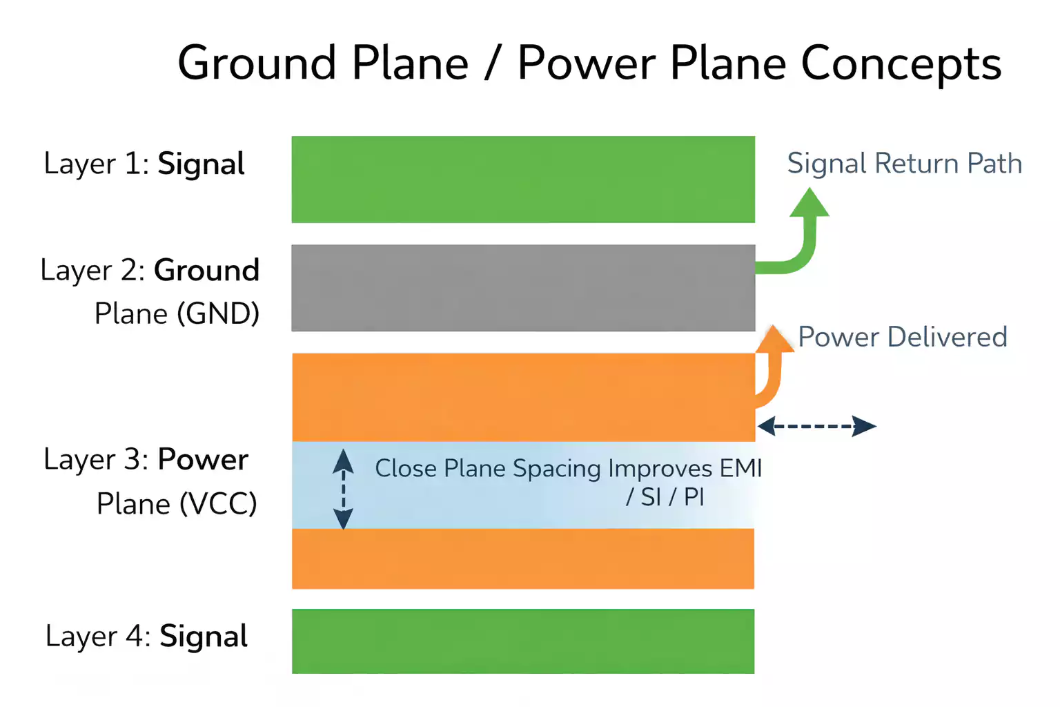
Think about return paths and grounding
A signal always has a return path, and that return path matters.
One of the most overlooked aspects of the PCB design layout is the grounding strategy. If possible, use a solid ground plane or a ground area to support signal return currents and reduce noise. When return paths are broken or forced to take long detours, the board is more likely to suffer from EMI, instability, or hard-to-diagnose strange behavior.
Even on a simple board, grounding choices can have a big impact. Avoid chopping the ground into isolated islands whenever possible, and try to keep return paths short and continuous.
Should you use the autorouter?
EAGLE includes autorouting tools, and it is tempting to let the software do the work. On a very simple board, that can sometimes be acceptable. But in most real designs, autorouting does not produce the best result.
Manual routing usually gives you much better control over power delivery, grounding, signal flow, and board readability. It also makes it easier to prioritize the nets that matter most.
PCB Layout Best Practices in EAGLE CAD
If you want better results, focus less on clicking commands and more on following good layout principles.
A few practical habits go a long way.
Set design rules early.
Do not wait until the board is finished to think about trace width, clearance, via size, and drill limits.
Verify footprints before routing.
A clean layout is meaningless if the actual parts do not fit.
Design for assembly.
Leave enough spacing between parts for soldering, inspection, and possible rework.
Keep silkscreen readable.
Reference designators, polarity marks, and connector labels should remain visible and useful.
Know your manufacturer’s limits.
Minimum trace width, minimum spacing, drill tolerance, and annular ring requirements all affect what can actually be built.
Match routing to the current function.
A low-current logic net and a power trace should not be treated the same way.
Step 5: Run DRC and Fix Layout Errors
Before exporting manufacturing files, run DRC (Design Rule Check). This is one of the most important quality-control steps in the entire process.
DRC helps identify problems such as:
- clearance violations
- traces that are too close together
- unrouted airwires
- overlapping pads or copper objects
- via or drill sizes outside limits
- silkscreen printed over pads
- Copper is placed too close to the board edge.
It is also worth doing a manual visual review. Software checks are important, but they do not always catch awkward connector orientation, poor part spacing, or labeling problems that a human eye will spot immediately.
Step 6: Export Gerber Files for PCB Manufacturing
Once the layout passes review, the last step is preparing the manufacturing output.
For most PCB fabrication jobs, you will need:
- Gerber files for copper, solder mask, silkscreen, and board outline
- NC drill files
- a BOM if assembly is involved
- pick-and-place data for automated assembly, if needed
A board is not truly finished when the routing is done. It is finished when it is ready to be manufactured without guesswork.
Common Beginner Mistakes in EAGLE CAD PCB Design
Many first-time PCB designers run into the same problems. Knowing them in advance can save a lot of time.
Using unverified footprints
This is one of the most common and most expensive mistakes.
Routing before placement is finalized
If the placement is weak, the routing will usually be weak too.
Making power traces too thin
Power delivery needs a proper trace width.
Putting decoupling capacitors too far away
That reduces their effectiveness and can create stability problems.
Relying too much on the autorouter
A fully connected board is not always a well-designed board.
Skipping ERC or DRC
That is a fast way to send avoidable mistakes into fabrication.
Conclusion
EAGLE CAD PCB design is not really about learning where the menus are. The bigger skill is knowing how to turn a clean schematic into a board that is logical, readable, and ready for manufacturing.
If you focus on the full process—schematic, placement, routing, rule checking, and Gerber export—you will build better boards and avoid many of the problems that slow beginners down.
And once your design is ready for prototyping or production, a reliable PCB manufacturer such as FastTurnPCB can help you move from design file to finished board with fewer delays and fewer surprises.
