
Power and ground planes are continuous copper layers in a multilayer PCB that provide low-impedance paths for power delivery, signal return, and shielding. A ground plane establishes a stable 0 V reference and helps reduce EMI, while a power plane distributes voltage more efficiently across the board. When kept continuous, closely spaced, and properly decoupled, these planes improve signal integrity, power integrity, and overall EMC performance.
In high-speed PCB design, many signal issues are not caused by the trace alone. They often come from poor return-path control, weak power distribution, split reference planes, or ineffective decoupling. That is why PCB ground plane and power plane design are essential to modern PCB layout.
In practice, power distribution, return paths, decoupling capacitors, and plane layout should be designed as one system. When done well, high-speed digital interfaces, analog front ends, and mixed-signal circuits become easier to route and more predictable in real hardware.
Key takeaways
- A solid ground plane provides a lower-impedance return path and helps reduce loop area.
- A well-designed PCB ground plane improves signal integrity, EMI control, and current return behavior.
- A power plane helps evenly distribute voltage, reduces voltage drop, and supports transient current demand.
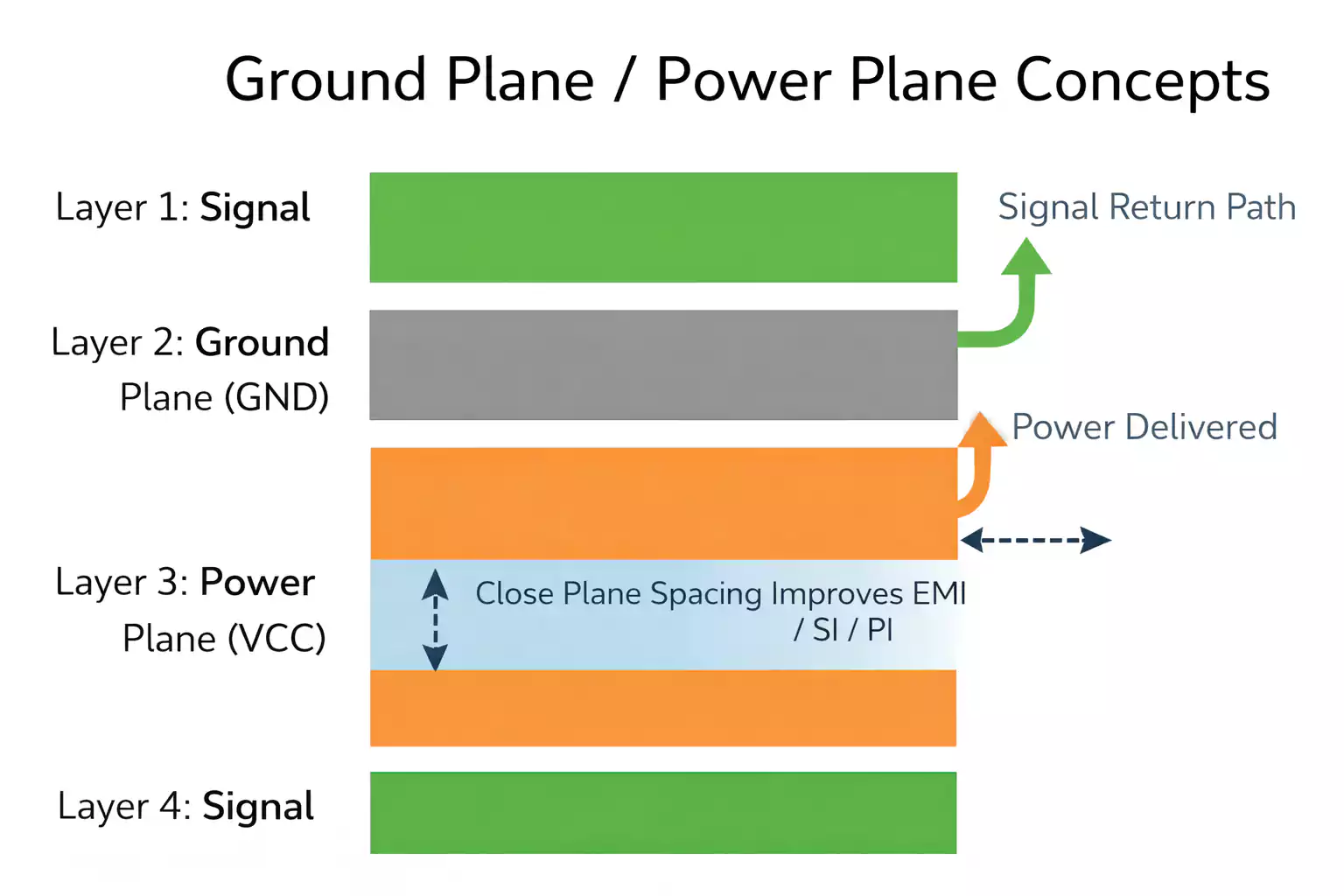
- In multilayer boards, keeping the power and ground planes adjacent reduces plane capacitance and improves high-frequency decoupling.
- In a 2-layer PCB ground-plane design, maintaining a continuous ground reference is usually more important than dedicating a full layer to power.
What is a PCB ground plane, and what is a power plane?
A PCB ground plane is a large, continuous copper area, often spanning the entire layer, connected to ground. It serves as the system's common electrical reference and provides the preferred return path for current. A power plane is a conductive layer used to distribute one or more supply voltages across the board. In multilayer designs, these planes reduce the need for long power and ground traces and can improve routing efficiency.
Beyond connectivity, planes also affect board-level performance. Ground planes help reduce noise and EMI by providing a low-impedance path for return currents, while power planes help deliver current more evenly and reduce voltage drop. Both can also improve thermal spreading because large copper areas help distribute heat across the board.
Why ground planes matter in high-speed PCB grounding
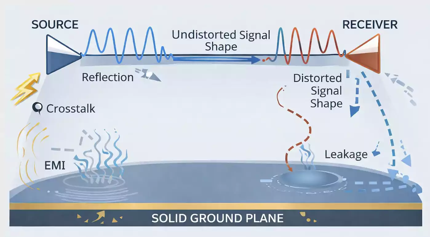
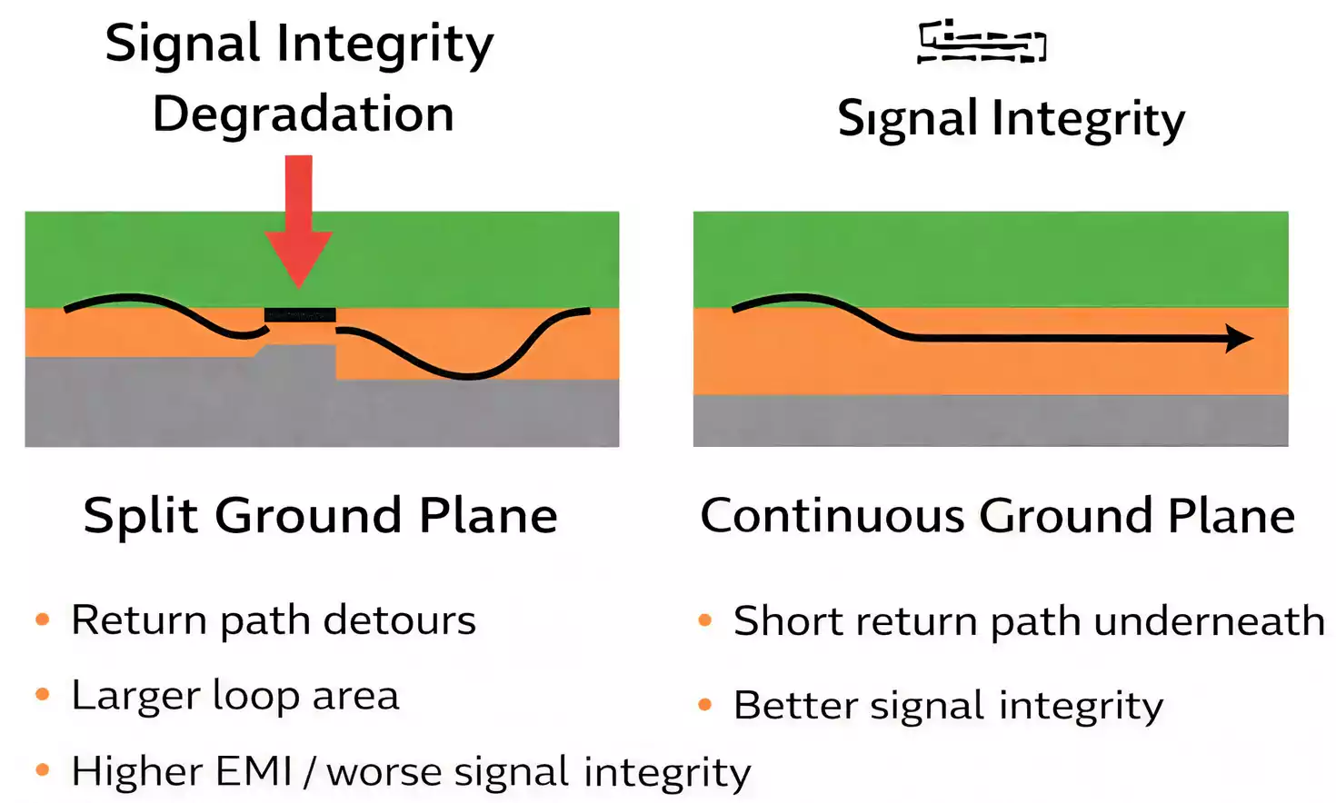
In high-speed PCB grounding, the return current path is just as important as the forward signal path. When a trace is routed over a solid reference plane, the return current tends to stay close to that trace, which minimizes loop area and reduces noise radiation. When the reference plane is split, missing, or too far away, the return current is forced to take a longer and less predictable path, increasing the risk of EMI, crosstalk, and signal degradation.
Engineers say the most important part of a fast signal is often the plane under it, not the trace. A continuous ground plane supports impedance control and stable signals.
Ground plane vs. power plane: what each one does
| Ground plane | Provides 0 V reference and return path | Helps reduce EMI, supports signal integrity, and stabilizes return current flow |
| Power plane | Distributes supply voltage | Reduces voltage drop, supports current delivery, and improves power distribution |
| Ground + power plane pair | Forms tightly coupled reference structure | Improves plane capacitance and high-frequency decoupling |
This distinction matters because the ground plane is usually the more critical plane for signal reference and return-path control, while the power plane primarily supports voltage distribution. In many stackups, if you have to prioritize one continuous plane, the ground plane should come first.
2-layer PCB ground plane vs. multilayer plane design
A 2-layer PCB ground plane can work for simpler, slower designs, but it is much harder to keep continuous because the same layers must handle routing, components, and the copper pour. That makes return-path control less predictable and usually forces power delivery to rely on traces instead of a dedicated power plane.
In contrast, multilayer boards make it much easier to dedicate one layer to a solid ground plane and another to a power plane. This improves routing density, keeps return paths short, and gives every signal layer a nearby reference plane. Thus, dedicated power planes are typical in four-layer and up.
A practical rule of thumb
- 2-layer PCB: prioritize a usable ground plane and route power with traces.
- 4-layer PCB and above: use a continuous ground plane, and add a power plane or power regions where needed.
Why return path control matters more than most designers expect
A high-speed signal is always a loop. Current leaves through the signal path and returns via the reference. With a solid plane beneath the trace, the return path is short and low inductance. Crossing a split plane, gap, or poor reference forces a detour, increasing loop area and EMI or signal-integrity risk.
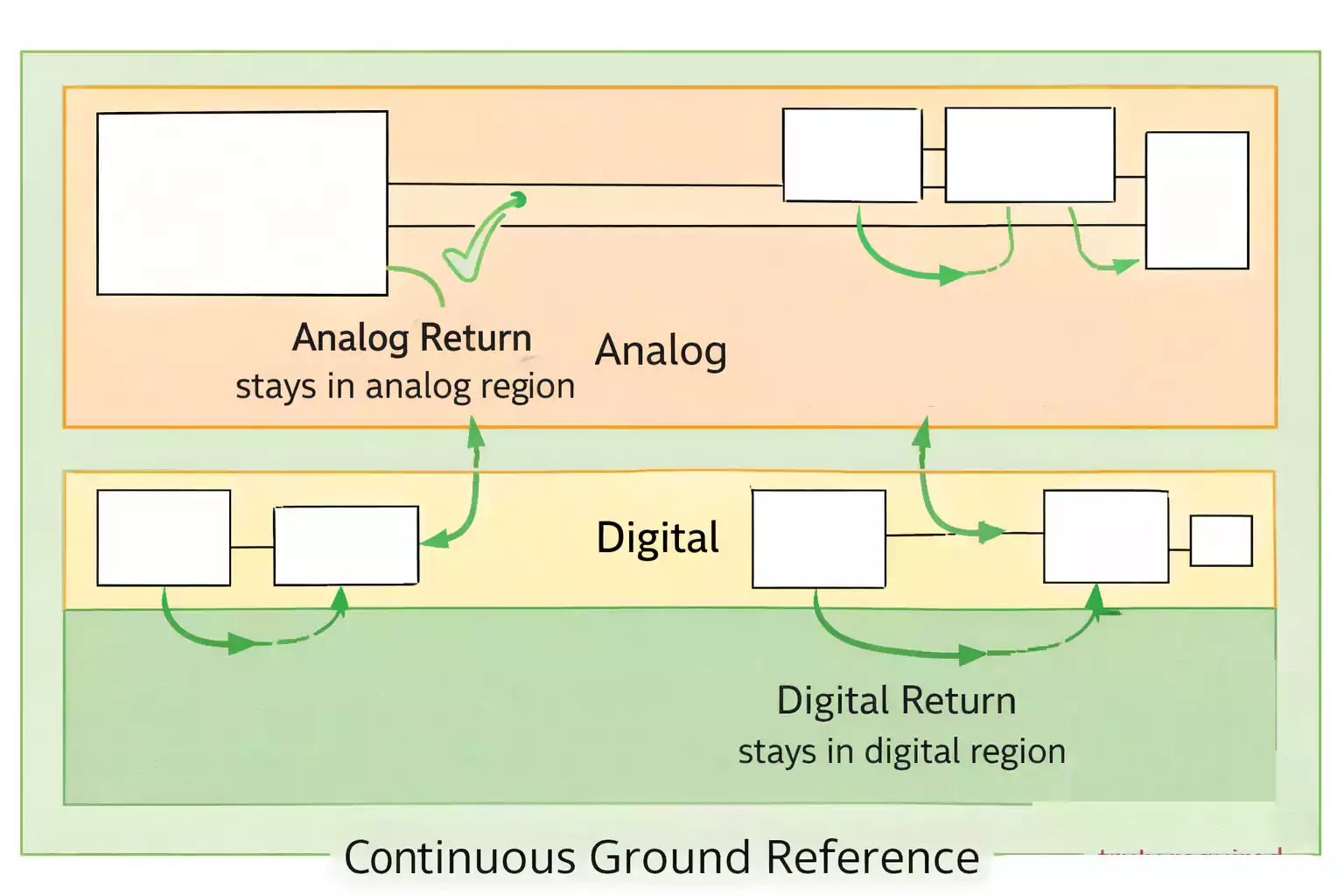
This is especially important in mixed-signal designs. Digital return currents should not flow through sensitive analog regions. The layout goal is not simply “separate analog and digital,” but to ensure each signal class has a clear, appropriate reference path.
Best practices for power plane and ground plane design
1. Keep the ground plane as continuous as possible
A continuous ground plane stabilizes references and reduces EMI. Avoid unnecessary splits, neck-downs, and large voids beneath high-speed traces, as these gaps can make impedance unpredictable.
2. Place power and ground planes adjacent
When power plane and ground plane layers sit next to each other, the dielectric spacing between them creates distributed capacitance. This improves high-frequency decoupling and helps lower PDN impedance. Thin dielectric spacing between those planes is commonly recommended for that reason.
3. Give every signal layer a clear reference plane
Every signal layer should reference a continuous plane above or below it, ideally a ground plane and secondarily a power plane. This is one of the most important stackup rules for controlling return current and impedance.
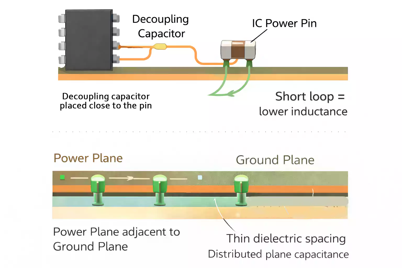
4. Keep decoupling capacitors close to the load
Decoupling capacitors should be placed close to IC power pins and tied to the power and ground planes with short, low-inductance connections. Using a mix of capacitor values helps cover a range of frequencies.
5. Use vias carefully, including via stitching where appropriate
Multiple vias can reduce inductance when connecting planes to pads and traces. Via stitching can also improve connectivity and EMI shielding, especially around critical regions. But vias also disturb copper planes, so they must be placed intentionally, especially near sensitive high-speed routes.
6. Split power domains only when needed
If the design requires different voltages, splitting a power plane into multiple domains may be useful. But domain splitting increases the risk of noise coupling, crosstalk, and return-path complications, so it should be done only with clear intent and strong EMC discipline.
Mixed-signal PCB ground plane considerations
In mixed-signal boards, the main objective is to keep digital noise from contaminating sensitive analog circuits. That does not necessarily mean physically splitting the ground plane everywhere. In fact, hard ground splits can create undefined return paths and often cause more problems than they solve.
A better approach is to maintain a solid ground reference, place analog and digital circuits thoughtfully, and control return-current paths. If separate AGND and DGND regions are needed, keep traces over their respective reference areas and carefully select ground connections to prevent return currents from crossing domains.
Common mistakes in PCB ground plane design
1. Routing high-speed traces over plane gaps
This breaks the intended return path and often causes reflection, radiation, and noise problems.
2. Treating the ground copper pour as the same as a true ground plane
A fragmented pour on a two-layer board is not equivalent to a continuous internal PCB ground plane.
3. Putting decoupling capacitors too far from the IC power pins
A capacitor that is electrically far away is much less effective at controlling fast transient current demand.
4. Prioritizing power plane completeness over ground plane continuity
In most high-speed layouts, a solid ground plane is more important than a full power plane.
5. Splitting analog and digital grounds without understanding return current
Ground separation without return-path planning can make mixed-signal behavior worse, not better.
Suggested stackup mindset
Instead of asking, “Where do I pour copper?” it is usually better to ask:
- Where does the signal current return?
- Does each signal layer have a continuous reference?
- Is the ground plane uninterrupted under critical traces?
- Are the power plane and ground layers close enough to support good decoupling?
- Are analog, digital, and high-current regions arranged so their return currents do not interfere with one another?
That mindset is closer to how experienced PCB designers evaluate real-world layout quality.
Conclusion
A PCB ground plane is not just a copper area tied to GND. It is the reference structure that defines signal return behavior, supports impedance control, reduces EMI, and stabilizes overall system performance. A power plane is not just a convenient way to distribute voltage; it is part of the board’s power integrity strategy and works best when paired thoughtfully with the ground system.
For high-speed designs, the most reliable approach is usually clear: keep the ground plane continuous, provide signals with a clean return path, place the power and ground layers close together, and support the stackup with proper decoupling. In a 2-layer PCB ground-plane design, that means being disciplined about copper continuity and return paths. On a multilayer board, it means using the stackup to your advantage from the beginning.