
Designing a reliable USB PCB used to be relatively straightforward. With USB 2.0, engineers focused on routing a single differential pair, keeping traces short, and ensuring basic impedance control. But with the widespread adoption of USB Type-C, PCB design has become significantly more complex.
A modern USB Type-C PCB supports high-speed differential signaling, reversible connector mapping, CC-based role detection, higher current, and strict EMI/ESD protection in compact layouts.
This guide walks through the essential layout and routing best practices for USB PCB design, with a focus on USB Type-C connectors. Whether you're designing a USB 2.0 device, a USB 3.x high-speed interface, or a Type-C port with power delivery support, these principles will help you avoid common design pitfalls and improve signal integrity.
USB Type-C vs. Traditional USB Connectors
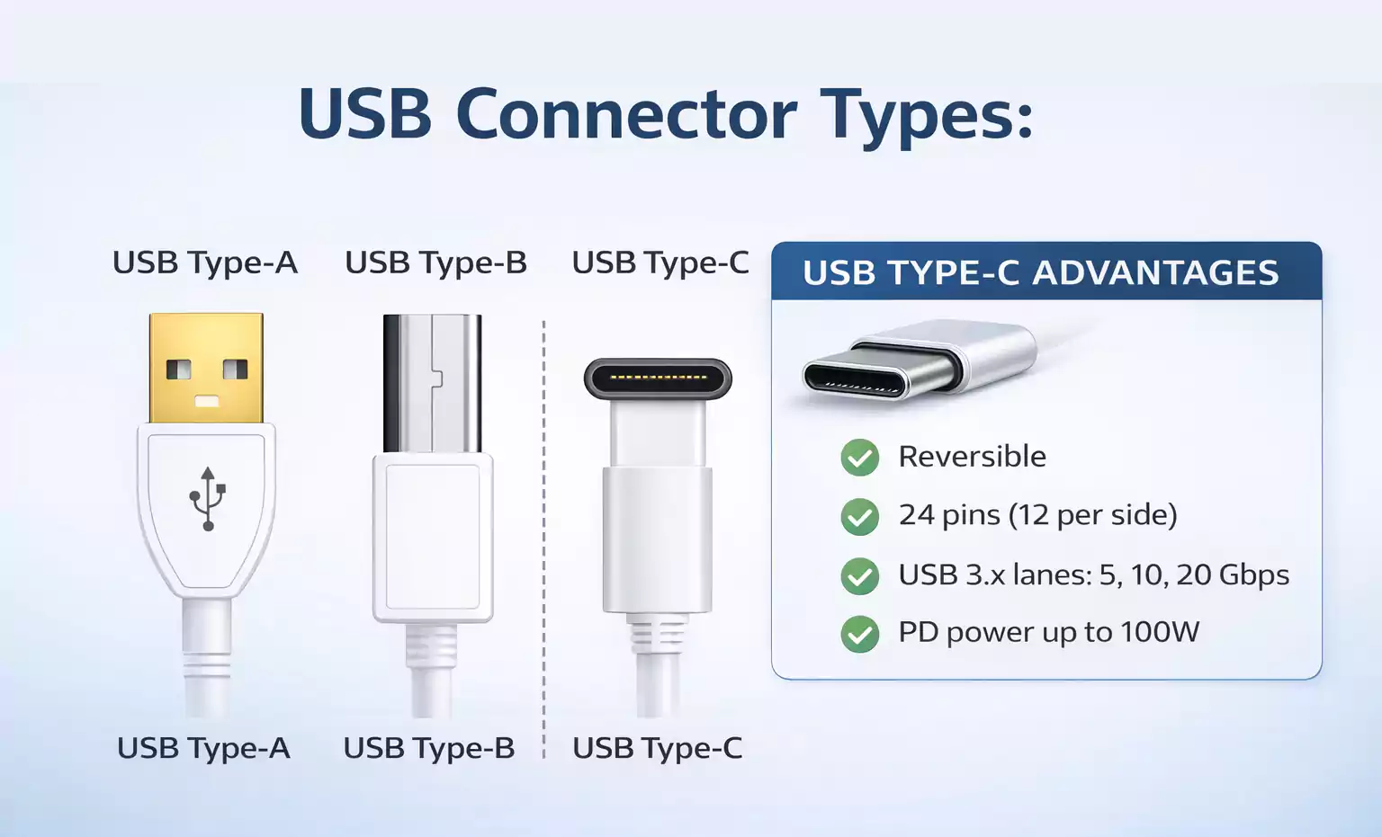
Unlike legacy USB Type-A or Micro-USB connectors, the USB Type-C connector features:
- A reversible plug orientation
- 24 pins arranged symmetrically
- Support for USB 2.0 and USB 3.x SuperSpeed signals
- Higher power capability through USB Power Delivery (PD)
- Additional sideband and configuration channels
This means your PCB layout must account for:
- Dense breakout routing
- Multiple differential pairs
- CC (Configuration Channel) logic
- Higher current VBUS traces
- Strict impedance control
A USB Type-C connector is a high-speed, multi-function subsystem, not just a physical interface.
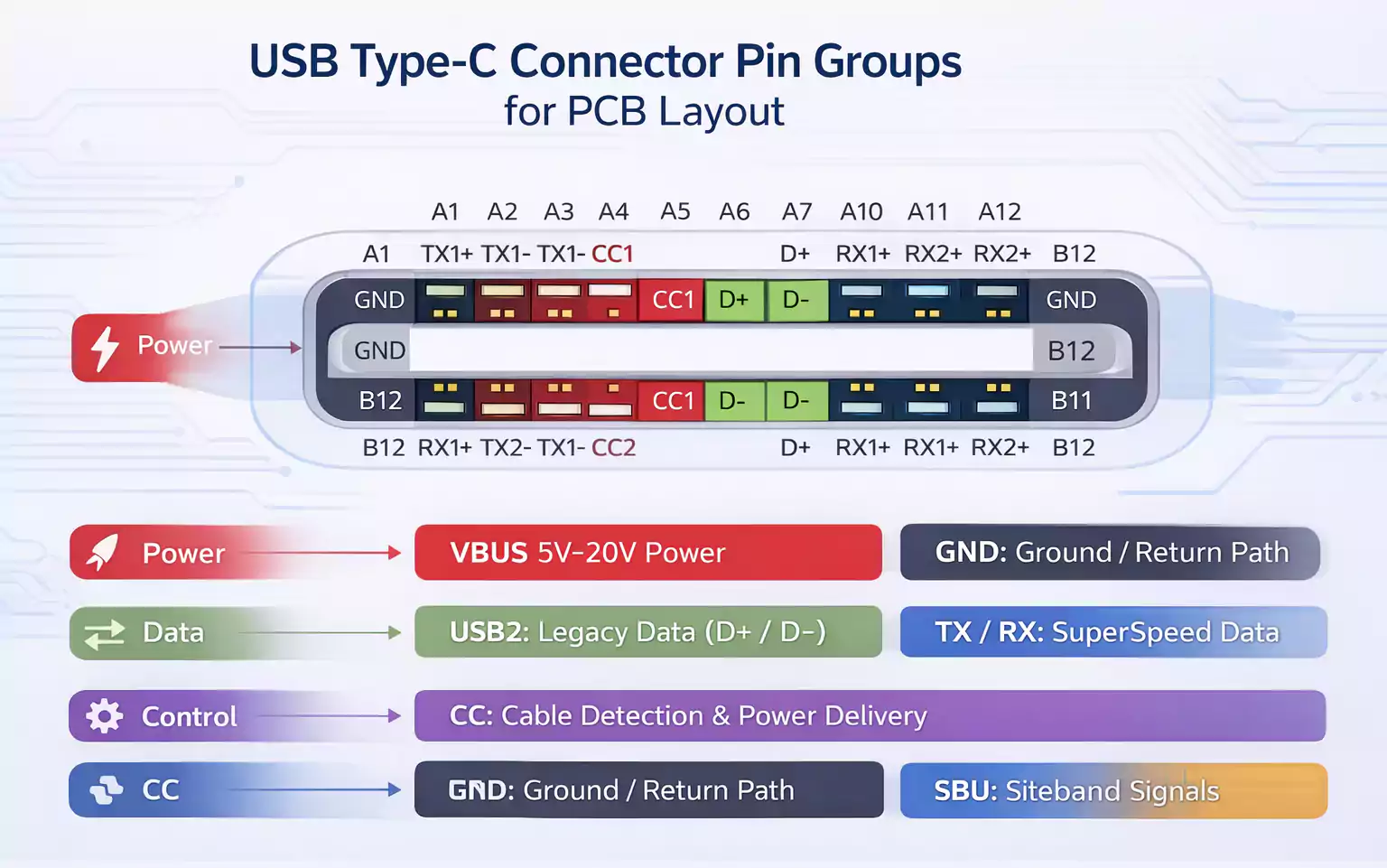
USB Type-C PCB Connector Pinout
Before starting layout, you must clearly understand the USB Type-C connector pin groups:
1. VBUS and GND
VBUS supplies 5V and, with PD, can support higher voltages and current levels. These traces must be wide enough to handle the current without excessive temperature rise or voltage drop.
2. USB 2.0 D+ and D−
These differential signals ensure backward compatibility. They require controlled differential impedance, typically 90Ω.
3. SuperSpeed Differential Pairs (USB 3.x)
These high-speed TX/RX pairs operate at multi-gigabit data rates and are highly sensitive to routing quality, impedance discontinuities, and via transitions.
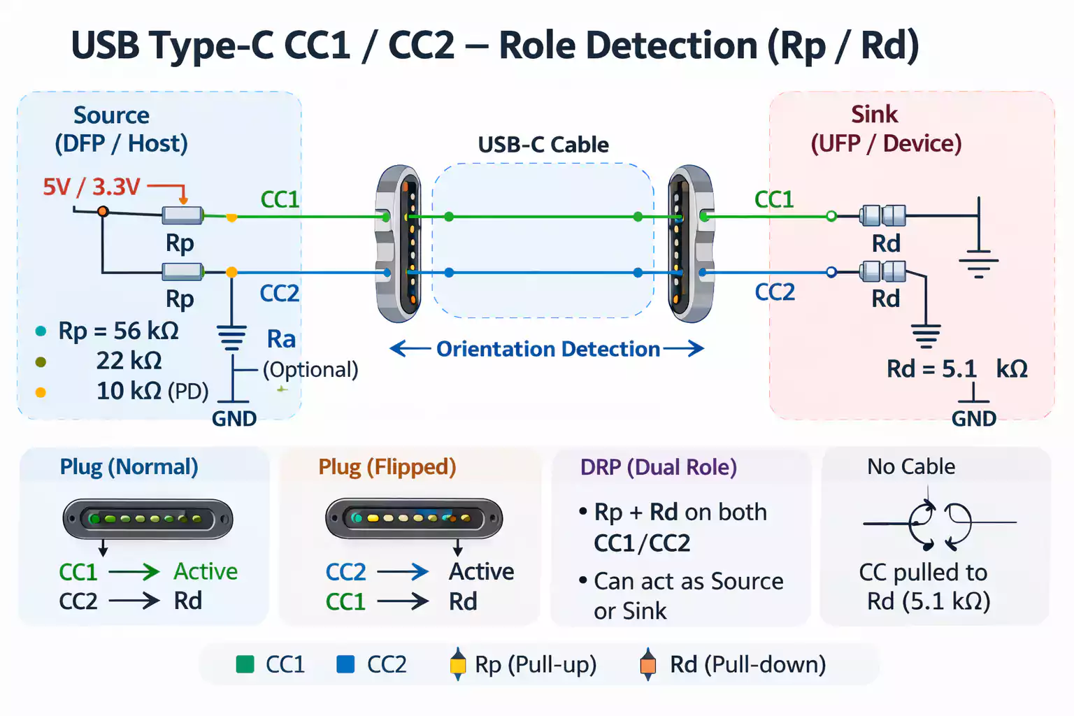
4. CC1 and CC2 (Configuration Channel Pins)
These pins perform:
- Cable orientation detection
- Source/Sink role identification
- Current advertisement
- USB Power Delivery communication
Incorrect CC routing can cause connection instability or improper power negotiation.
CC Pin Design Considerations
The CC pins are not differential signals; treat them as single-ended lines. However, they must still be routed carefully.
Key guidelines include:
- Avoid routing near noisy switching power circuits.
- Maintain a clean ground reference.
- Keep routing short and direct.
- Ensure proper pull-up (Rp) or pull-down (Rd) resistor configuration based on Source, Sink, or Dual-Role design.
For simple power-only Type-C ports, a basic resistor configuration may be sufficient. However, for full USB Power Delivery functionality, a dedicated PD controller is strongly recommended.
USB Type-C Connector Placement on PCB
The Type-C connector should be positioned close to the PCB edge to allow mechanical clearance for plug insertion. Ensure:
- Adequate keep-out space
- Strong mechanical support
- Reinforced ground pads for durability
- Proper anchoring to withstand repeated insertion cycles
Mechanical reliability is just as important as signal integrity.
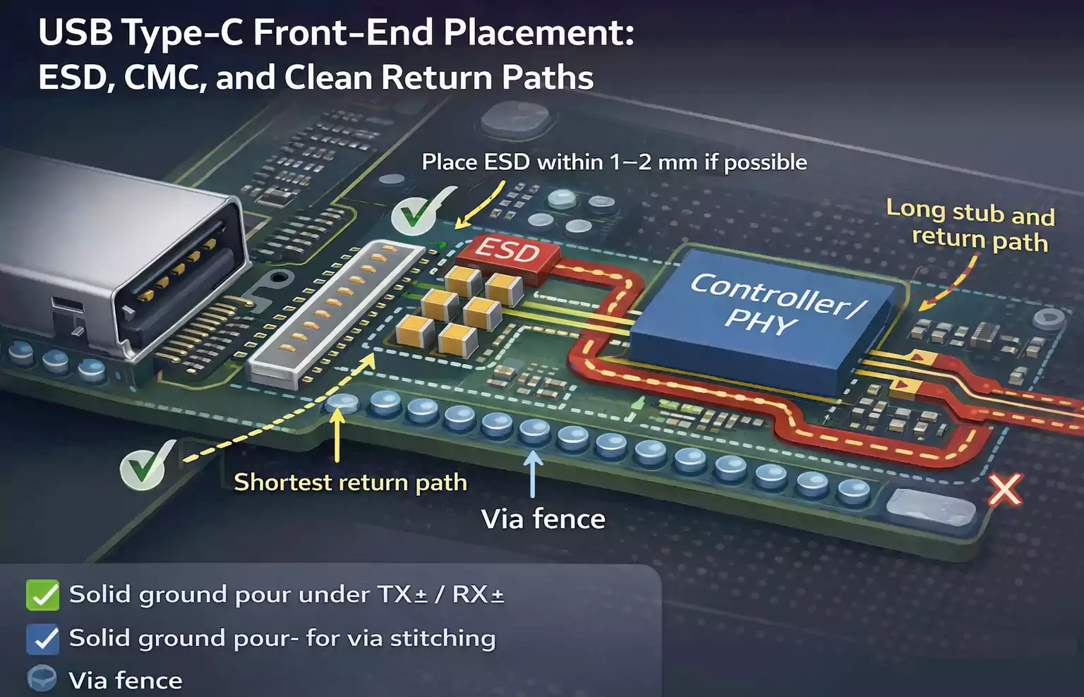
ESD Protection and Common-Mode Choke Placement
One of the most critical layout areas is the region immediately behind the connector.
Recommended signal chain order:
Connector → ESD Protection → Common-Mode Choke → Controller
Best practices:
- Place ESD diodes as close to the connector pins as possible.
- Minimize trace length between the connector and the protection devices.
- Maintain low-inductance grounding for ESD return paths.
- Avoid long stubs between protection components.
If common-mode chokes are used, ensure they are placed after ESD devices and maintain symmetric routing.
AC Coupling Capacitor Placement
For USB 3.x SuperSpeed lanes, AC coupling capacitors are typically required.
Placement rules:
- Place TX coupling capacitors near the transmitter side (often close to the connector in device designs).
- Maintain symmetry between differential lines.
- Avoid long trace stubs around capacitors.
- Ensure impedance continuity through capacitor pads.
Improper capacitor placement can introduce impedance discontinuities and degrade signal quality.
USB Differential Pair Routing Guidelines
1. USB 2.0 Routing Requirements
USB 2.0 differential pairs require:
- 90Ω differential impedance
- Short and direct routing
- Minimal vias
- Avoidance of 90-degree corners
- Consistent trace spacing
Length matching should be controlled to prevent excessive skew between D+ and D−.
2. USB 3.x SuperSpeed Routing Requirements
USB 3.x significantly raises the bar for PCB layout.
Key rules include:
- Maintain 90Ω differential impedance with tighter tolerance.
- Keep routing on the same layer whenever possible.
- Minimize via transitions.
- Maintain pair symmetry.
- Avoid stubs and discontinuities.
- Keep trace geometry consistent.
At multi-gigabit speeds, even small discontinuities can degrade eye diagrams and reduce signal margin.
Differential Pair Length Matching
Length matching is important—but it must not override good routing practices.
Best practices:
- Keep differential pairs as short as possible.
- Match lengths within the pair.
- Avoid excessive serpentine tuning.
- Do not sacrifice reference plane integrity just to achieve perfect length numbers.
Over-tuning can introduce impedance variation and degrade performance.
Spacing and Crosstalk Control
To reduce crosstalk:
- Maintain sufficient spacing between adjacent differential pairs.
- Keep USB lanes away from high-frequency clock signals.
- Avoid routing parallel to switching power traces.
- Use solid ground shielding between sensitive signals if necessary.
Spacing requirements depend on stackup and signal layer configuration.
Ground Plane Design and Return Path Control
A continuous ground reference plane beneath USB differential traces is essential.
Avoid:
- Routing across plane splits.
- Crossing gaps or voids.
- Referencing different planes without return path stitching.
When signals transition layers, ensure return path continuity by placing nearby ground vias. This minimizes loop area and reduces EMI.
Return path control is often overlooked, but it directly affects impedance stability and electromagnetic emissions.
Via Usage and Layer Transitions
Every via introduces parasitic inductance and capacitance.
Guidelines:
- Minimize via count in high-speed lanes.
- Keep differential vias symmetric.
- Limit the number of layer transitions.
- Avoid unnecessary stubs.
- If possible, use back-drilling for high-speed designs.
In USB 2.0 designs, limited vias may be acceptable. In USB 3.x and beyond, each via must be justified.
Common USB Type-C PCB Design Mistakes
1. Treating Type-C Like Legacy USB
Designers sometimes reuse old USB 2.0 routing strategies for Type-C connectors. This can cause:
- Impedance mismatches
- Signal integrity issues
- EMI failures
2. Ignoring CC Pin Layout
Improper CC routing can result in:
- Incorrect orientation detection
- Inconsistent charging behavior
- Power negotiation failure
3. Routing Across Split Planes
This causes:
- Return path discontinuity
- Impedance variation
- Increased radiation
4. Placing ESD Too Far From the Connector
This reduces protection effectiveness and increases the risk of damage to downstream ICs.
5. Overusing Vias in SuperSpeed Pairs
Excessive vias introduce reflections and degrade signal integrity.
USB Power Considerations in Type-C Designs
Even if your primary focus is data routing, VBUS must not be overlooked.
For high-current designs:
- Use wide copper pours for VBUS.
- Analyze voltage drop.
- Ensure adequate copper thickness.
- Provide proper thermal dissipation.
- Validate the connector's current rating.
If implementing USB Power Delivery:
- Integrate a PD controller.
- Protect VBUS with OVP and OCP.
- Consider thermal stress near the connector.
Type-C ports reliably support both data and power.
Final Design Review Checklist
Before sending your USB PCB for fabrication:
- Confirm impedance calculations match the stackup.
- Verify continuous ground reference under all high-speed lanes.
- Check ESD device proximity and grounding.
- Validate CC resistor configuration.
- Review differential pair length and symmetry.
- Confirm minimal via transitions.
- Ensure VBUS copper width supports the target current.
- Inspect breakout routing from connector pads.
A disciplined review process prevents costly re-spins.
Conclusion
USB Type-C PCB design demands more than simple differential routing. It requires a comprehensive understanding of connector pinout, CC functionality, impedance control, differential-pair symmetry, return-path continuity, ESD strategy, and power-delivery considerations.
If you need help with USB PCB layout, high-speed routing, impedance control, or DFM, partnering with an experienced PCB manufacturer can reduce re-spins and shorten development cycles.
FastTurnPCB provides impedance-controlled fabrication and production-ready manufacturing for high-speed USB Type-C PCBs.
Build it right the first time—so your USB interface performs reliably in the real world.