


Maintaining signal integrity has become one of the most critical challenges in modern electronics. As data rates climb into the gigahertz range and edge transitions become faster, even short traces in a custom PCB can behave like transmission lines. When that happens, uncontrolled impedance variations can cause reflections, loss, timing errors, and electromagnetic interference (EMI).
That’s where controlled impedance PCBs come in.
This guide gives you a practical, engineer-friendly understanding of:
- When controlled impedance is actually required
- How to design and route controlled impedance traces
- How to specify your requirements clearly to a PCB manufacturer
- How impedance is verified in production
- Common mistakes that lead to failed builds, extra costs, and redesigns
Whether you're designing a high-speed digital interface, RF circuitry, or a product undergoing FCC/EMC testing, this is the comprehensive reference you need.
What Is a Controlled Impedance PCB?
A controlled impedance PCB is a printed circuit board designed so that specific traces maintain a predetermined electrical impedance—commonly 50 Ω for single-ended lines and 90 Ω or 100 Ω for differential pairs.
Impedance is not the same as resistance.
It reflects the AC opposition to current at high frequencies, influenced by both:
- the trace geometry (width, thickness, spacing)
- the dielectric properties and thicknesses of the PCB materials
In short, impedance stability matters because:
- At high frequencies, every trace becomes a transmission line.
- If the impedance suddenly rises or falls along its path, a portion of the signal is reflected.
- These reflections distort waveforms, degrade timing margins, and increase EMI.
A controlled-impedance PCB ensures the signal experiences a consistent electrical environment from driver to receiver.
When Do You Need Controlled Impedance?
Not every trace on a PCB requires impedance control. However, if your system includes high-speed or high-frequency signals, impedance stability becomes essential.
1. You likely need controlled impedance when working with:
- High-speed digital interfaces: PCIe, DDR, HDMI, USB 3.x, Ethernet (1G/2.5G/10G), SATA
- RF and microwave systems (cellular, radar, GNSS, low-noise amplifiers, power amplifiers)
- Differential signaling (LVDS, USB differential pairs, high-speed SerDes)
- Longer routing distances, where the trace delay becomes significant
- Low-noise analog front ends that require consistent line impedance.
- Products undergoing EMI/EMC compliance testing
2. You may not need controlled impedance when:
- Signals operate at very low frequencies (kHz to low MHz)
- Trace lengths are extremely short.
- The signal is not edge-speed sensitive.
- Drivers and receivers do not require matched impedance per the datasheet.
Common Controlled Impedance Structures
Different routing layers and geometries result in different impedance behaviors. The most common structures include:
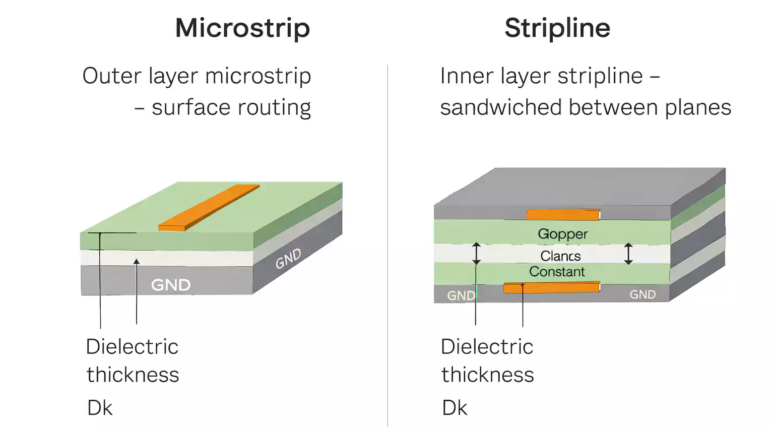
1. Microstrip (Outer Layer Routing)
A microstrip is a trace routed on an outer layer with a reference plane directly underneath it.
- Lower EMI shielding
- Easier to access and rework.
- Impedance affected by solder mask thickness
2. Stripline (Inner Layer Routing)
A stripline is sandwiched between two reference planes.
- Great isolation
- More consistent impedance
- Typically requires smaller trace widths to achieve the same target impedance.
3. Differential Pairs
Two traces carrying equal and opposite signals.
Impedance depends on:
- individual trace geometry
- spacing between the traces
- symmetry (VERY important)
4. Coplanar Waveguide (CPW)
Uses ground pours adjacent to the trace.
Useful for:
- RF designs
- Tight impedance control
- Routing in dense boards
Understanding these structures helps determine appropriate trace width, spacing, and stack-up.
What Affects PCB Controlled Impedance?
Several geometric and material parameters determine whether a trace meets its target impedance.
1. Trace Width
Wider traces lower impedance; narrower traces raise it.
2. Trace Spacing (for differential pairs)
- Smaller spacing leads to stronger coupling and lower differential impedance.
- Larger spacing reduces coupling and raises differential impedance.
3. Copper Thickness
Thicker copper lowers impedance.
(1 oz copper often requires wider lines to hit 50Ω than 0.5 oz copper.)
4. Dielectric Thickness (Height to Reference Plane)
The farther the trace is from the ground plane, the higher the impedance.
5. Dielectric Constant (Dk / Er)
High-frequency materials with lower Dk (e.g., Rogers) generally exhibit higher impedance for the same geometry than FR-4.
6. Reference Plane Continuity
Crossing a gap or slot in the reference plane causes immediate impedance discontinuities, increasing reflections and EMI.
7. Manufacturing Tolerances
Even with perfect design, copper etching, prepreg thickness variation, and resin content introduce slight impedance variation — typically ±10% unless a tighter spec is negotiated.
Controlled Impedance PCB Design Workflow
A reliable approach to controlled impedance starts long before you route the first trace.
Step 1 — Identify Which Nets Require Controlled Impedance
Review chip datasheets and interface requirements.
Identify:
- differential pairs
- high-speed serial nets
- clock nets
- RF paths
Step 2 — Define the Stack-Up Before Routing
Your impedance depends heavily on:
- number of layers
- signal layer location
- copper thickness
- dielectric thickness
- material type (FR-4, high-Tg, low-loss, PTFE, Rogers, etc.)
Do not begin routing until the stack-up is locked.
Step 3 — Calculate Trace Width and Spacing
Use a field solver or impedance calculator that supports:
- microstrip/stripline
- differential impedance
- CPW
- solder mask effects
Each layer may require a different width to hit 50Ω/100Ω.
Step 4 — Annotate Requirements Clearly
Add impedance notes to your:
- schematic
- layer stack manager
- fabrication notes
- Gerber readme or drawing package
Make it clear which nets need controlled impedance and their target values.
Step 5 — Review With SI/DFM Before Release
Check for:
- reference plane gaps
- excessive via transitions
- mismatched lengths
- sudden geometry changes
- inconsistent spacing
A short pre-fabrication review prevents costly rework.
Controlled Impedance Routing Best Practices
Routing is where many designs lose impedance control. These rules help ensure your layout performs as expected.
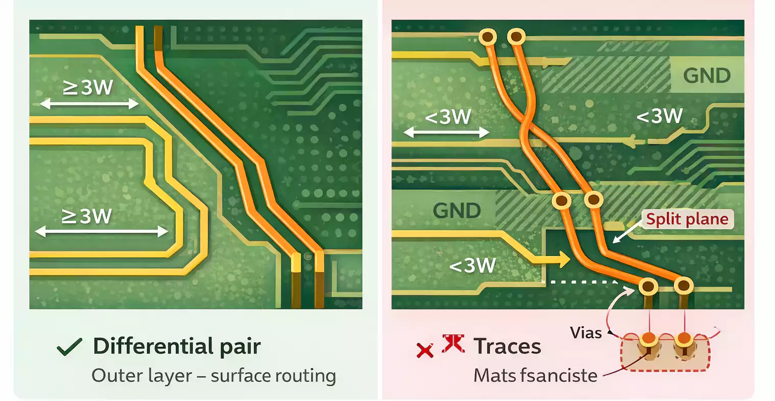
1. Keep Differential Pairs Symmetrical
Maintain:
- equal trace widths
- equal spacing
- parallel paths
- matched lengths
Symmetry is essential for suppressing common-mode noise.
2. Maintain Proper Spacing From Other Signals
General guidelines:
- Keep other traces at least 3W away (three times the trace width)
- For very sensitive differential pairs, use 5W spacing.
This minimizes crosstalk.
3. Avoid Crossing Split Planes or Gaps
Crossing an internal plane split forces the return current to take a longer path, causing:
- reflections
- EMI radiation
- timing issues
Always provide a continuous reference plane.
4. Minimize Via Transitions
Each via introduces a small impedance bump.
If layer changes are unavoidable, keep the number of vias consistent between pair members.
5. Match Differential Pair Lengths
Offset length compensation should be placed close to the imbalance source.
Avoid serpentine routing in areas with strong coupling to other nets.
6. Use Unique Line Widths for Controlled Impedance Traces
A subtle but highly effective practice:
Choose a width like 5.1 mil instead of 5.0 mil.
It helps your manufacturer instantly identify controlled-impedance nets during CAM review.
How Controlled Impedance Is Verified in Manufacturing
PCB manufacturers verify impedance through test coupons, not the signal traces themselves.
1. Test Coupons
Coupons duplicate the geometry of your controlled impedance traces and are placed on the panel edge for testing.
2. TDR (Time Domain Reflectometry)
A fast electrical pulse is injected through the coupon, and reflections reveal whether the trace hits the target impedance.
3. When VNA Is Used
Vector Network Analyzers are used mainly for higher-frequency RF applications.
4. Why Only Coupons Are Tested
Measuring actual signal traces would require cutting into your board.
Coupons offer an identical structure without damaging the product.
Common Mistakes to Avoid
- Starting Routing Before the Stack-Up Is Finalized
- Not Specifying Which Nets Need Controlled Impedance
- Conflicting Notes Across Files
- Setting Unrealistic Tolerances
- Placing Vias or Components Between Differential Pair Members
- Crossing Plane Splits
FAQ
Do all high-speed traces need controlled impedance?
No. Only signals where reflections impact performance—typically high-speed serial interfaces, clocks, RF lines, or differential pairs.
What is the difference between single-ended and differential impedance?
Single-ended impedance is measured to the reference plane.
Differential impedance is measured between two complementary traces.
Can the PCB manufacturer adjust trace width?
Yes, if you explicitly allow it. Many designers give the manufacturer permission to fine-tune widths based on their exact materials and equipment.
What tolerance should I choose?
±10% is standard.
±5% requires specialized processes and may increase cost.
What is the difference between controlled dielectric and controlled impedance?
Controlled dielectric means you precisely control the thickness of the material stack.
Controlled impedance means the manufacturer tunes geometry to hit a target impedance using their own field solver and testing.
Final Thoughts
Controlled impedance is no longer just a concern for RF specialists—it’s now essential for nearly every modern digital and communication product. With the right stack-up planning, routing discipline, and clear communication with your PCB vendor, controlled impedance becomes a predictable and manageable part of your design workflow.
If you need reliable custom-controlled impedance PCB fabrication, FastTurnPCB offers expert DFM support, quick-turn production, and precise impedance testing to help your design perform exactly as intended.
